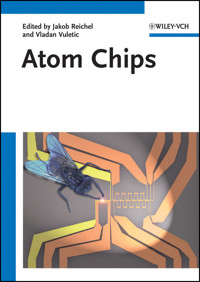
Atom Chips E-Book
129,99 €
Mehr erfahren.
- Herausgeber: Wiley-VCH
- Kategorie: Wissenschaft und neue Technologien
- Sprache: Englisch
This stimulating discussion of a rapidly developing field is divided into two parts. The first features tutorials in textbook style providing self-contained introductions to the various areas relevant to atom chip research.
Part II contains research reviews that provide an integrated account of the current state in an active area of research where atom chips are employed, and explore possible routes of future progress. Depending on the subject, the length of the review and the relative weight of the 'review' and 'outlook' parts vary, since the authors include their own personal view and style in their accounts.
Sie lesen das E-Book in den Legimi-Apps auf:
Seitenzahl: 889
Veröffentlichungsjahr: 2011
Ähnliche
Contents
Preface
List Of Contributors
PART ONE: FUNDAMENTALS
1 FROM MAGNETIC MIRRORS TO ATOM CHIPS
ANDREI SIDOROV AND PETER HANNAFORD
1.1 INTRODUCTION
1.2 HISTORICAL BACKGROUND
1.3 MAGNETIC MIRRORS FOR COLD ATOMS
1.4 THE MAGNETIC FILM ATOM CHIP
1.5 PERMANENT MAGNETIC LATTICE ON A MAGNETIC FILM ATOM CHIP
1.6 SUMMARY AND CONCLUSIONS
REFERENCES
2 TRAPPING AND MANIPULATING ATOMS ON CHIPS
JAKOB REICHEL
2.1 INTRODUCTION
2.2 OVERVIEW OF TRAPPING TECHNIQUES
2.3 MAGNETIC TRAPS FOR NEUTRAL ATOMS
2.4 THE DESIGN OF WIRE PATTERNS FOR MAGNETIC POTENTIALS
2.5 REAL WIRES: ROUGHNESS AND MAXIMUM CURRENT
2.6 LOADING TECHNIQUES
2.7 VACUUM CELLS
2.8 CONCLUSION AND OUTLOOK
REFERENCES
3 ATOM CHIP FABRICATION
RON FOLMAN, PHILIPP TREUTLEIN AND JÖRG SCHMIEDMAYER
3.1 INTRODUCTION
3.2 FABRICATION CHALLENGES
3.3 THE SUBSTRATE
3.4 LITHOGRAPHY
3.5 METALLIC LAYERS
3.6 ADDITIONAL FEATURES
3.7 CURRENT DENSITIES AND TESTS
3.8 PHOTONICS ON ATOM CHIPS
3.9 CHIP DICING, MOUNTING, AND BONDING
3.10 FURTHER INTEGRATION AND PORTABILITY
3.11 CONCLUSION AND OUTLOOK
REFERENCES
PART TWO: ULTRACOLD ATOMS NEAR A SURFACE
4 ATOMS AT MICROMETER DISTANCES FROM A MACROSCOPIC BODY
STEFAN SCHEEL AND E.A. HINDS
4.1 INTRODUCTION
4.2 PRINCIPLES OF QED IN DIELECTRICS
4.3 RELAXATION RATES NEAR A SURFACE
4.4 CASIMIR–POLDER FORCES
4.5 CLOSING REMARKS
REFERENCES
5 INTERACTION OF ATOMS, IONS, AND MOLECULES WITH SURFACES
CARSTEN HENKEL
INTRODUCTION
5.1 QUALITATIVE OVERVIEW
5.2 INTERACTION POTENTIALS
5.3 SURFACE-INDUCED ATOMIC TRANSITIONS
5.4 PERSPECTIVES
REFERENCES
PART THREE: COHERENCE ON ATOM CHIPS
6 DIFFRACTION AND INTERFERENCE OF A BOSE–EINSTEIN CONDENSATE SCATTERED FROM AN ATOM CHIP-BASED MAGNETIC LATTICE
A. GÜNTHER, T.E. JUDD, J. FORTÁGH AND C. ZIMMERMANN
6.1 INTRODUCTION
6.2 EXPERIMENTAL SETUP
6.3 THE MAGNETIC LATTICE POTENTIAL
6.4 DIFFRACTION AND INTERFERENCE
6.5 BALLISTIC EXPANSION AND PHASE IMPRINTING
6.6 EXPERIMENTAL RESULTS
6.7 EFFECT OF ATOMIC INTERACTIONS
6.8 CONCLUSION
REFERENCES
7 INTERFEROMETRY WITH BOSE–EINSTEIN CONDENSATES ON ATOM CHIPS
THORSTEN SCHUMM, STEPHANIE MANZ, ROBERT BÜCKER, DAVID A. SMITH AND JÖRG SCHMIEDMAYER
7.1 INTRODUCTION
7.2 ATOM CHIP BEC SPLITTERS BASED ON STATIC FIELDS
7.3 ATOM CHIP BEC SPLITTERS BASED ON DRESSED ADIABATIC POTENTIALS
7.4 MATTER–WAVE INTERFEROMETRY WITH BOSE–EINSTEIN CONDENSATES
7.5 INTERFEROMETRY WITH 1D QUASI CONDENSATES
7.6 SUMMARY AND OUTLOOK
REFERENCES
8 MICROCHIP-BASED TRAPPED-ATOM CLOCKS
VLADAN VULETIĆ, IAN D. LEROUX AND MONIKA H. SCHLEIER-SMITH
8.1 BASIC PRINCIPLES
8.2 ATOMIC-FOUNTAIN VERSUS TRAPPED-ATOM CLOCKS
8.3 OPTICAL-TRANSITION CLOCKS VERSUS MICROWAVE CLOCKS
8.4 CLOCKS WITH MAGNETICALLY TRAPPED ATOMS: FUNDAMENTAL LIMITS TO PERFORMANCE
8.5 CLOCKS WITH MAGNETICALLY TRAPPED ATOMS: EXPERIMENTAL DEMONSTRATIONS
8.6 READOUT IN TRAPPED-ATOM CLOCKS
8.7 SPIN SQUEEZING
REFERENCES
9 QUANTUM INFORMATION PROCESSING WITH ATOM CHIPS
PHILIPP TREUTLEIN, ANTONIO NEGRETTI AND TOMMASO CALARCO
9.1 INTRODUCTION
9.2 INGREDIENTS FOR QIP WITH ATOM CHIPS
9.3 QUBIT STATES WITH LONG COHERENCE LIFETIME
9.4 QUBIT ROTATIONS (SINGLE-QUBIT GATES)
9.5 SINGLE-QUBIT READOUT (SINGLE-ATOM DETECTION)
9.6 SINGLE-QUBIT PREPARATION (SINGLE-ATOM PREPARATION)
9.7 CONDITIONAL DYNAMICS (TWO-QUBIT GATES)
9.8 HYBRID APPROACHES TO QIP ON A CHIP
9.9 CONCLUSION AND OUTLOOK
REFERENCES
PART FOUR: NEW DIRECTIONS
10 CRYOGENIC ATOM CHIPS
GILLES NOGUES, ADRIAN LUPAŞCU, ANDREAS EMMERT, MICHEL BRUNE, JEAN-MICHEL RAIMOND AND SERGE HAROCHE
10.1 INTRODUCTION
10.2 SUPERCONDUCTING ATOM CHIP SETUP: SIMILARITIES AND DIFFERENCES WITH CONVENTIONAL ATOM CHIPS
10.3 PERSPECTIVES FOR CRYOGENIC ATOM CHIPS: A NEW REALM OF INVESTIGATIONS
10.4 CONCLUSION
REFERENCES
11 ATOM CHIPS AND ONE-DIMENSIONAL BOSE GASES
I. BOUCHOULE, N.J. VAN DRUTEN AND C.I. WESTBROOK
11.1 INTRODUCTION
11.2 REGIMES OF ONE-DIMENSIONAL GASES
11.3 1D GASES IN THE REAL WORLD
11.4 EXPERIMENTS
11.5 CONCLUSION
REFERENCES
12 FERMIONS ON ATOM CHIPS
MARCIUS H.T. EXTAVOUR, LINDSAY J. LEBLANC, JASON MCKEEVER, ALMA B. BARDON, SETH AUBIN, STEFAN MYRSKOG, THORSTEN SCHUMM AND JOSEPH H. THYWISSEN
12.1 INTRODUCTION
12.2 THEORY OF IDEAL FERMI GASES
12.3 THE ATOM CHIP
12.4 LOADING THE MICROTRAP
12.5 RAPID SYMPATHETIC COOLING OF A K-RB MIXTURE
12.6 SPECIES-SELECTIVE RF MANIPULATION
12.7 FERMIONS IN AN OPTICAL DIPOLE TRAP NEAR AN ATOM CHIP
12.8 DISCUSSION AND FUTURE OUTLOOK
REFERENCES
13 MICRO-FABRICATED CHIP TRAPS FOR IONS
J.M. AMINI, J. BRITTON, D. LEIBFRIED AND D.J. WINELAND
13.1 INTRODUCTION
13.2 RADIO-FREQUENCY ION TRAPS
13.3 DESIGN CONSIDERATIONS FOR PAUL TRAPS
13.4 MEASURING HEATING RATES
13.5 MULTIPLE TRAPPING ZONES
13.6 TRAP MODELING
13.7 TRAP EXAMPLES
13.8 FUTURE
REFERENCES
Index
Related Titles
Stolze, J., Suter, D.Quantum ComputingA Short Course from Theory to Experiment2008ISBN: 978-3-527-40787-3
Matta, C.F., Boyd, R.J. (eds.)The Quantum Theory of Atoms in MoleculesFrom Solid State to DNA and Drug Design2007ISBN: 978-3-527-30748-7
Bruß, D., Leuchs, G. (eds.)Lectures on Quantum Information2007ISBN: 978-3-527-40527-5
Vogel, W., Welsch, D.-G.Quantum Optics2006ISBN: 978-3-527-40507-7
Bachor,H.-A., Ralph,T.C.A Guide to Experiments in Quantum Optics2004ISBN: 978-3-527-40393-6
Weidemüller, M., Zimmermann, C. (eds.)Interactions in Ultracold GasesFrom Atoms to Molecules2009ISBN: 978-3-527-40750-7
Leuchs, G., Beth,T.(eds.)Quantum Information Processing2003ISBN: 978-3-527-40371-4
Cohen-Tannoudji, C., Dupont-Roc, J., Grynberg, G.Atom-Photon InteractionsBasic Processes and Applications1998ISBN: 978-0-471-29336-1
The Editors
Prof. Jakob ReicheLaboratoire Kastler Brossel de l’E.N.S. 24, rue Lhomond 75231 Paris Cedex 05 Frankreich
Prof. Vladan VuletiMassachusetts Inst. of Technology, Room 26-231 77, Massachusetts Avenue Cambridge, MA 02139-4309 USA
All books published by Wiley-VCH are carefully produced. Nevertheless, authors, editors, and publisher do not warrant the information contained in these books, including this book, to be free of errors. Readers are advised to keep in mind that statements, data, illustrations, procedural details or other items may inadvertently be inaccurate.
Library of Congress Card No.: applied for
British Library Cataloguing-in-Publication Data: A catalogue record for this book is available from the British Library.
Bibliographic information published by the Deutsche Nationalbibliothek The Deutsche Nationalbibliothek lists this publication in the Deutsche Nationalbibliografie; detailed bibliographic data are available on the Internet at http://dnb.d-nb.de.
© 2011 WILEY-VCH Verlag GmbH & Co. KGaA, Boschstr. 12, 69469 Weinheim, Germany
All rights reserved (including those of translation into other languages). No part of this book may be reproduced in any form – by photoprinting, microfilm, or any other means – nor transmitted or translated into a machine language without written permission from the publishers. Registered names, trademarks, etc. used in this book, even when not specifically marked as such, are not to be considered unprotected by law.
Preface
This book intends to give both an introduction and an in-depth review of the beautiful physics being done with atom chips. Topics range from the manipulation of single atoms to the quantum entanglement between many atoms, and from interferometry with atomic matter waves to studies of fundamental atom–surface interactions.
For about three decades researchers have used magnetic and electric fields from DC to optical frequencies to confine neutral atoms for a variety of experiments and applications. The term atom chip has come to designate setups where microscopic or micro-fabricated structures, typically confined to a surface, generate three-dimensional trapping fields in the vicinity of the surface.
At its inception, the atom chip was regarded primarily as a tool to conveniently generate electromagnetic fields varying on a small length scale, and as such is related to early prototypes of magnetic mirrors. In fact, the attainment of Bose–Einstein condensation on a chip in 2001 in Tübingen and Munich was the first landmark that brought atom chips to the attention of the physics community at large. Since then, a growing number of research groups has adopted microchips as a convenient and fast method for the creation of Bose–Einstein condensates (BECs), and now also degenerate Fermi gases.
The strongly confining, complex, multi-parameter potentials that can be realized with atom chips have enabled experimentalists to explore new situations. For example, studies of one-dimensional quantum gases are benefitting from extremely elongated single traps that can be generated on atom chips, and BECs have been diffracted from specifically designed magnetic lattices realized on the chip surface.
However, atom chips are not merely devices to form atom traps by a combination of conductors and insulators on a surface. Atom chips promise rich functionality and integrability, and possibly nano-scale miniaturization, as advertised early on by a number of researchers in the field. The small length scale well matched to the condensate size and proximity of a solid surface have opened up and driven further research possibilities. The first and perhaps most immediate example is the investigation of fundamental surface-induced forces, such as the van der Waals and Casimir–Polder forces. This field has progressed and expanded considerably due to the close and stimulating interaction between atom chip experimentalists and theorists. Furthermore, the repertoire of fields and interactions used on atom chips has grown to include radiofrequency and microwave potentials, resonant and fardetuned optical fields in miniature optical devices, as well as surface interactions with micro-mechanical structures. In each case, the small-scale, near-field situation of the atom chip has been exploited in ingenious ways to create new and rich physical situations that go beyond the possibilities of macroscopic experiments. Examples include coupling of a BEC to an oscillating mechanical cantilever, cavity quantum electrodynamics experiments with BECs, and some of the most beautiful condensate interferometry experiments performed so far.
The combination of these features makes atom chips an interesting platform for quantum information and quantum simulation experiments. This has also motivated the development of the newest family of atom chips, surface-electrode-based ion traps, which present both similarities and interesting differences compared to their neutral-atom counterparts.
A third area has emerged where atom chips are used as a means to construct the most compact and robust ultra-cold atom devices. The very recent demonstration of BEC in microgravity was enabled by an atom chip. Trapped-atom clocks on atom chips are being explored as promising secondary frequency standards. The idea of “integrated atom optics” on atom chips as a means to build atom interferometers emerged with the first atom chip experiments, but is certainly still in its infancy today. Last but not least, experiments with BECs in cryogenic environments also benefit from the small size and robustness of atom chips.
This book represents a collective effort by the community of atom chip researchers to outline the state of their knowledge as of 2009/2010. Each chapter starts with a thorough introduction before exposing the state of the art on a specific topic. Additionally, there are introductory chapters describing the particularities of designing magnetic potentials and producing BECs on atom chips, as well as on atom chip fabrication. The latter is discussed in a tutorial style and sufficient detail to enable a researcher with minimal micro-fabrication knowledge to start fabricating atom chips. In this way, we hope that the book will be valuable for students and researchers who are entering the field of atom chips or are active in one of the neighboring fields, but also for anyone desiring to get an overview of this beautiful and active area of contemporary quantum physics.
Paris and Cambridge, June 2010Jakob Reichel and Vladan Vuletić
List of Contributors
Jason M. AminiSignature Technology Laboratory Georgia Technology Research Institute 400 Tenth Street Atlanta, GA 30318 USA
Seth AubinDepartment of Physics College of William and Mary Williamsburg, VA 23185 USA
Alma B. BardonDepartment of Physics University of Toronto 60 St. George Street Toronto, Ontario M5S 1A7 Canada
Isabelle BouchouleLaboratoire Charles Fabry de l’Institut d’Optique Campus Polytechnique RD 128 91127 Palaiseau Cedex France
Joe BrittonTime and Frequency Division National Institute of Standards and Technology 325 Broadway Boulder, CO 80305 USA
Michel BruneLaboratoire Kastler Brossel de l’E.N.S. 24, rue Lhomond 75231 Paris Cedex 05 France
Robert BückerAtominstitut der Österreichischen Universitäten TU Wien Stadionallee 2 1020 Wien Austria
Tommaso CalarcoInstitut für Quanteninformationsverarbeitung Universität Ulm Albert-Einstein-Allee 11 89069 Ulm Germany
Andreas EmmertLaboratoire Kastler Brossel de l’E.N.S. 24, rue Lhomond 75231 Paris Cedex 05 France
Marcius H.T.ExtavourOntario Power Generation 700 University Avenue Toronto, Ontario Canada, M5G 1X6
Ron FolmanAtom Chip Group Ben-Gurion University Be’er Sheva, 84105 Israel
József FortághPhysikalisches Institut Universität Tübingen Auf der Morgenstelle 14 72076 Tübingen Germany
A. GüntherPhysikalisches Institut Universität Tübingen Auf der Morgenstelle 14 72076 Tübingen Germany
Peter HannafordCentre for Atom Optics & Ultrafast Spectroscopy Faculty of Engineering and Industrial Science Swinburne University of Technology Serpells Lane, Mail H38, PO Box 218 Hawthorn, Victoria 3122 Australia
Serge HarocheLaboratoire Kastler Brossel de l’E.N.S. 24, rue Lhomond 75231 Paris Cedex 05 France
Carsten HenkelInstitut für Physik und Astronomie Campus Golm Universität Potsdam 14476 Potsdam Germany
Edward A. HindsCentre for Cold Matter Blackett Laboratory Imperial College London Prince Consort Road London SW7 2AZ United Kingdom
Thomas E. JuddPhysikalisches Institut Universität Tübingen Auf der Morgenstelle 14 72076 Tübingen Germany
Lindsay J. LeBlancDepartment of Physics University of Toronto 60 St. George Street Toronto, Ontario M5S 1A7 Canada
Dietrich LeibfriedTime and Frequency Division National Institute of Standards and Technology 325 Broadway Boulder, CO 80305 USA
Ian D. LerouxMIT Department of Physics 77 Massachusetts Avenue Cambridge, MA 02139 USA
Adrian LupaşcuInstitute for Quantum Computing University of Waterloo 200 University Ave. W. Waterloo, ON N2L 3G1 Canada
Stephanie ManzAtominstitut der Österreichischen Universitäten TU Wien Stadionallee 2 1020 Wien Austria
Jason McKeeverEntanglement Technologies Palo Alto, CA 94306 USA
Stefan MyrskogMorgan Solar Inc. 30 Ordnance St. Toronto, Ontario M6K 1A2 Canada
Antonio NegrettiInstitut für Quanteninformationsverarbeitung Universität Ulm Albert-Einstein-Allee 11 89069 Ulm Germany
Gilles NoguesInstitut Neel 25 avenue des Martyrs bâtiment T, BP 166 38042 Grenoble cedex 9
Jean-Michel RaimondLaboratoire Kastler Brossel de l’E.N.S. 24, rue Lhomond 75231 Paris Cedex 05 France
Jakob ReichelLaboratoire Kastler Brossel de l’E.N.S. 24, rue Lhomond 75231 Paris Cedex 05 France
Stefan ScheelBlackett Laboratory Imperial College London Prince Consort Road London SW7 2AZ United Kingdom
Monika H. Schleier-SmithMIT Department of Physics 77 Massachusetts Avenue Cambridge, MA 02139 USA
Jörg SchmiedmayerAtominstitut der Oesterreichischen Universitäten TU Wien Stadionallee 2 1020 Vienna Austria
Thorsten SchummAtominstitut der Österreichischen Universitäten TU Wien Stadionallee 2 1020 Wien Austria
Andrei SidorovCentre for Atom Optics & Ultrafast Spectroscopy Faculty of Engineering and Industrial Science Swinburne University of Technology Serpells Lane, Mail H38, PO Box 218 Hawthorn, Victoria 3122 Australia
David A. SmithAtominstitut der Österreichischen Universitäten TU Wien Stadionallee 2 1020 Wien Austria
Joseph H. ThywissenDepartment of Physics University of Toronto 60 St. George Street Toronto, Ontario M5S 1A7 Canada
Philipp TreutleinUniversity of Basel Department of Physics Klingelbergstrasse 82 CH-4056 Basel Switzerland
N. J. (Klaasjan) van DrutenVan der Waals-Zeeman Instituut Universiteit van Amsterdam Valckenierstraat 65-67 1018 XE Amsterdam Netherlands
Vladan VuletićMIT Department of Physics 77 Massachusetts Avenue Cambridge, MA 02139 USA
Christopher I. WestbrookLaboratoire Charles Fabry de l’Institut d’Optique Campus Polytechnique RD 128 91127 Palaiseau Cedex France
David J. WinelandTime and Frequency Division National Institute of Standards and Technology 325 Broadway Boulder, CO 80305 USA
C. ZimmermannPhysikalisches Institut Universität Tübingen Auf der Morgenstelle 14 72076 Tübingen Germany
PART ONE
FUNDAMENTALS
1
FROM MAGNETIC MIRRORS TO ATOM CHIPS1)
Andrei Sidorov and Peter Hannaford
1.1 Introduction
Following the advent of laser cooling and trapping techniques in the 1980s, a new exciting area of research, ‘atom chips’, has emerged in which sophisticated micron-scale structures on planar substrates are produced utilizing the latest technological developments in lithography and nanofabrication. These complex microstructures produce tiny magnetic field configurations which can trap, cool, and manipulate ensembles of ultra-cold atoms in the vicinity of a surface. Scaling down the dimensions of atom trapping geometry offers extended possibilities for the production and control of Bose–Einstein condensates (BECs). Enormous progress on the generation of BECs and quantum degenerate Fermi gases, on-chip matter–wave interferometers, and integrated detectors has been made in the last few years.
In the second section of this article we trace the historical evolution of this new field, from the first surface-based atom optical elements – magnetic mirrors – to the present-day micro-fabricated structures on a substrate – atom chips. In Section 1.3 we present the basic principles of magnetic mirrors for cold atoms and describe different types of magnetic mirror. Section 1.4 describes the production of a BEC on a permanent magnetic film atom chip; the application of this atom chip to probe the topology of magnetic fields using RF spectroscopy and to study the adiabatic splitting of a BEC in a double well for sensing asymmetric potentials; and investigations of the spatially dependent relative phase evolution of a two-component BEC. Finally, in Section 1.5 we describe a permanent magnetic lattice on an atom chip for trapping and manipulating multiple arrays of ultra-cold atoms and quantum degenerate gases.
1.2 Historical Background
In 1983 Opat [1] proposed the idea of using periodic arrays of electric fields on a planar substrate to reflect beams of polar molecules in a matter–wave interferometer. Almost a decade later the Melbourne group [2] reported the reflection of a beam of chloromethane (CH3Cl) molecules from the exponentially decaying electric field above a periodic array of electrodes of alternating polarity.2) Opat and coworkers [3] then extended these ideas to periodic arrays of magnetic fields to create a surface-based mirror for reflecting beams of laser-cooled atoms (Figure 1.1a). As slowly moving atoms in positive (or ‘low-field seeking’) magnetic states approach the periodic magnetic structure they experience an exponentially increasing magnetic field, with decay length a/2π (where a is the period), and for sufficiently large magnetic fields the atoms are repelled by the structure. A number of schemes [3] were proposed for producing the periodic magnetic structures, including the use of arrays of magnets of alternating polarity, periodic magnetic fields ‘recorded’ on ferromagnetic substrates as in sound recording, and planar arrays of parallel wires alternately carrying electric current in opposite directions. Methods for fabricating the surface-based microstructures were suggested including lithographical techniques used in the electronics industry.
Figure 1.1 Schematic diagram of (a) a magnetic mirror consisting of perpendicularly magnetized elements of alternating polarity, (b) a grooved perpendicularly magnetized microstructure [10].
The first magnetic mirror for cold atoms was realized in 1995 by Roach et al. [4] by recording sinusoidal signals onto a magnetic audio-tape and observing the retroflection of laser-cooled rubidium atoms from the recorded structure. Soon after, Sidorov et al. [5] in Melbourne reported the retroreflection of cold cesium atoms from a 2-mm-period planar array of Nd-Fe-B magnets of alternating polarity. In 1997 the Sussex group demonstrated the focusing and multiple reflection of cold atoms bouncing on a curved magnetic mirror made from a concave-shaped floppy disk or video tape [6, 7].
One of the major challenges was to be able to scale the magnetic structures down to micron-scale periods, in order to produce a hard mirror with very short decay length and minimal finite-size effects. This problem was basically solved when it was shown [8] that a grooved periodic magnetic structure produces a magnetic field distribution that is essentially the same as that above an array of magnets of alternating polarity. The Melbourne group subsequently demonstrated the specular reflection of cold atoms from a 1-μm-period magnetic mirror constructed from micro-fabricated grooved structures coated with perpendicularly magnetized film [9, 10]. The scaling down of the period to 1 μm represented a significant advance in the miniaturization of surface-based atom optical elements.
In 1999 the Melbourne [11] and Harvard/Orsay/Gaithersburg [12] groups reported a magnetic mirror for cold atoms constructed from a planar array of current-carrying conductors lithographically patterned on a silicon wafer or a sapphire substrate. A feature of this type of magnetic mirror is that the magnetic field may be readily varied, switched or modulated by varying the current in the conductors. Such magnetic mirrors were the first micro-fabricated surface-based optical elements for cold atoms and represented a significant step towards the development of more sophisticated atom chips based on micro-fabricated current-carrying conductors on a substrate [13–15].
Lesen Sie weiter in der vollständigen Ausgabe!
Lesen Sie weiter in der vollständigen Ausgabe!
Lesen Sie weiter in der vollständigen Ausgabe!
Lesen Sie weiter in der vollständigen Ausgabe!
Lesen Sie weiter in der vollständigen Ausgabe!
Lesen Sie weiter in der vollständigen Ausgabe!
Lesen Sie weiter in der vollständigen Ausgabe!
Lesen Sie weiter in der vollständigen Ausgabe!
Lesen Sie weiter in der vollständigen Ausgabe!
Lesen Sie weiter in der vollständigen Ausgabe!
Lesen Sie weiter in der vollständigen Ausgabe!
Lesen Sie weiter in der vollständigen Ausgabe!
Lesen Sie weiter in der vollständigen Ausgabe!
Lesen Sie weiter in der vollständigen Ausgabe!
Lesen Sie weiter in der vollständigen Ausgabe!
Lesen Sie weiter in der vollständigen Ausgabe!


