Table of Contents
BENTHAM SCIENCE PUBLISHERS LTD.
End User License Agreement (for non-institutional, personal use)
Usage Rules:
Disclaimer:
Limitation of Liability:
General:
Foreword
PREFACE
List of Contributors
Photonic Crystal Instruments
Abstract
INTRODUCTION
PC SENSING INSTRUMENTS
PC OPTICAL LOGIC GATES
PC OPTICAL POWER SPLITTER AND POL. SPLITTER
PC POLARIZATION MAINTAINING INSTRUMENTS
PC BASED LASERS
CONCLUDING REMARKS
CONSENT FOR PUBLICATION
CONFLICT OF INTEREST
ACKNOWLEDGEMENT
REFERENCES
All-optical Logic Gate Using Photonic Crystals for Ultra-Fast Telecommunication Applications
Abstract
INTRODUCTION
RELATED WORKS
LIGHT PROPAGATION IN PERIODIC MEDIA
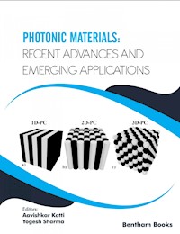
TYPES OF PHOTONIC CRYSTALS
1D PhC
2D PhC
3D PhC
PRINCIPLE OF OPERATION
PWE Method
Solutions of Maxwell’s Equations in Frequency Domain
FDTD Method
DESIGN OF PROPOSED ALL-OPTICAL XOR LOGIC GATE
PROPOSED ALL-OPTICAL XOR LOGIC GATE USING NANORESONATORS
CONCLUSION
CONSENT FOR PUBLICATION
CONFLICT OF INTEREST
ACKNOWLEDGEMENT
REFERENCES
Pressure Dependent Reflectance and Transmitt- ance Properties in 1D- Photonic Crystal Containing Germanium (Ge)
Abstract
INTRODUCTION
THEORETICAL MODEL
RESULTS AND DISCUSSION
Effect of Hydrostatic Pressure on Reflectance Properties of Normal PC Structure
Effect of Hydrostatic Pressure on the Transmission mode of Conjugate PC Structure
CONCLUSION
CONSENT FOR PUBLICATION
CONFLICT OF INTEREST
ACKNOWLEDGEMENT
REFERENCES
Recent Advances in Graphene Based Plasmonics
Abstract
INTRODUCTION
THEORETICAL FRAMEWORK OF PLASMONS IN GRAPHENE
Electronic Structure of Graphene
Optical Response and Dispersion Relation of Graphene Surface Plasmons
Semi-classical Model
Random Phase Approximation(RPA)
TYPES OF GRAPHENE SURFACE PLASMONS
COUPLING OF SURFACE PLASMONS WITH PHOTONS, PHONONS AND ELECTRONS
BEHAVIOUR OF SURFACE PLASMONS IN GRAPHENE WITH DIFFERENT DIMENSIONALITIES
Characteristics of Surface Plasmons in 2D Bilayer Graphene
Characteristics of Surface Plasmons in 1D Graphene Nanoribbons (GNRs) and 0D Graphene Quantum Dots (GQDs)
CURRENT APPLICATIONS OF SURFACE PLASMONS IN GRAPHENE
CONCLUSIONS AND FUTURE PERSPECTIVES
CONSENT FOR PUBLICATION
CONFLICT OF INTEREST
ACKNOWLEDGEMENTS
REFERENCES
Third Generation Solar Cells - Promising Devices to Meet the Future Energy Needs
Abstract
INTRODUCTION
Basic Parameters
Third Generation Solar Cells
Organic Solar Cells
Main Features of Conjugated Polymers
Principle of Operation
Perovskite Solar Cells
Dye Sensitized Solar Cells (DSSCs)
Quantum Dot Solar Cells
CONCLUSION
CONSENT FOR PUBLICATION
CONFLICT OF INTEREST
ACKNOWLEDGEMENTS
REFERENCES
Recent Advances of Graphene in Solar Cell Applications
Abstract
INTRODUCTION
APPLICATION OF GR IN VARIOUS TYPES OF SOLAR CELLS
Gr in Heterojunction Silicon Solar Cell
Graphene in Dye-Sensitized Solar Cells
Graphene in Perovskite Solar Cells
Graphene in Other Types of Solar cells
CONCLUSION
ABBREVIATIONS
CONSENT FOR PUBLICATION
CONFLICT OF INTEREST
ACKNOWLEDGEMENT
REFERENCES
A Review on the Materials and Applications of Nanophotonics
Abstract
INTRODUCTION
Materials
Two-dimensional Materials
Single Layered Graphene
Transition Metal Dichalcogenides
Photonic Crystals
Dielectric Nanostructures
Fabrication Techniques
Top-down Methods
Bottom-up Methods
APPLICATIONS
Absorbers
Graphene Photodetectors
2D TMDCs Based LEDs
Biosensing
CONCLUSION
CONSENT FOR PUBLICATION
CONFLICT OF INTEREST
ACKNOWLEDGEMENT
REFERENCES
Revolutionary Future Using the Ultimate Potential of Nanophotonics
Abstract
INTRODUCTION
Photons and Electrons: Similarities and Differences
Photons and Electrons: The Constriction in Various Facets
Propagation of sub-atomic Particles through a Classically Forbidden Zone
Localization Under a Periodic Potential
Nanoscale Optical Interactions
Axial Nanoscopic Localization
Evanescent Wave
Lateral Nanoscopic Localization
Quantum Confinement
Nanoscopic Interaction Dynamics
New Cooperative Transitions
Applications
Synchronous Oscillations of Delocalized Electrons on Nanoparticles and Surfaces
Fluorescence-Based Systems
Semiconductor Nanocrystals: Single-photon Sources
Semiconductor Nanocrystals: New Fluorescent Labels for Biology
Nano-Based Semiconductor Crystals: a New Active Component for Excimer Lasers
Organic Light Emitting Diode
DISCUSSION
CONCLUSION
CONSENT FOR PUBLICATION
CONFLICT OF INTEREST
ACKNOWLEDGEMENT
REFERENCES
A Simulative Study on Electro-Optic Character- istics of InAlGaAs/InP for Fiber Optic-based Communications under Nanoscale Well Thickness Layers
Abstract
INTRODUCTION
SIMULATED HETEROINTERFACE NANOSTRUCTURE, AND THEORETICAL DETAILS
COMPUTATIONAL RESULTS AND DISCUSSION
CONCLUSION
CONSENT FOR PUBLICATION
CONFLICT OF INTEREST
ACKNOWLEDGMENTS
REFERENCES
Two-Dimensional Materials for Advancement of Fiber Laser Technologies
Abstract
INTRODUCTION
2D Material-Based Saturable Absorbers for Fiber Lasers
2D Chalcogenides
Metal Monochalcogenides (MMs)
Transition Metal Dichalcogenides (TMDs)
MXenes
OPERATING PRINCIPLES FOR PULSE GENERATION IN FIBER LASER TECHNOLOGY
Q-switching Technique
Mode-locking Technique
CONFIGURATION OF 2D MATERIALS AS SATURABLE ABSORBERS
GENERATION OF Q-SWITCHED PULSES IN FIBER
The 1.0 μm Wavelength Region
The 1.5 μm Wavelength Region
The 2.0 μm Wavelength Region
GENERATION OF MODE-LOCKED PULSES IN FIBER LASERS
The 1.0 μm Wavelength Region
The 1.5 μm Wavelength Region
The 2.0 μm Wavelength Region
CONCLUSION, CHALLENGES, AND FUTURE PERSPECTIVES
CONSENT FOR PUBLICATION
CONFLICT OF INTEREST
ACKNOWLEDGEMENT
REFERENCES
Optical Properties of Hollow-Core Bragg Fiber Waveguides
Abstract
INTRODUCTION AND MOTIVATION
THEORETICAL MODELLING OF THE PROPOSED STRUCTURE
HANKEL FORMALISM OF THE PROPOSED STRUCTURE
NUMERICAL RESULTS AND DISCUSSION
CONCLUSION
CONSENT FOR PUBLICATION
CONFLICT OF INTEREST
ACKNOWLEDGEMENT
REFERENCES
Photonic Nanostructured Bragg Fuel Adulteration Sensor
Abstract
INTRODUCTION
MODELLING OF THE BFW PHOTONIC NANOSTRUCTURE
Hankel Function Formalism (HFF) and Transfer Matrix Methodology (TMM) in Cylindrical Coordinates
Various Predictive Models
Fuel Energy Adulteration Sensor Performance Parameter
NUMERICAL RESULTS AND DISCUSSION
CONCLUSION
CONSENT FOR PUBLICATION
CONFLICT OF INTEREST
ACKNOWLEDGEMENT
REFERENCES
Modelling Fabrication Variability in Silicon Photonic Devices.
Abstract
INTRODUCTION
PHOTONIC DEVICE LEVEL OPTIMIZATION
Iterative Optimisation Algorithms
Empirical Optimisation Algorithms
QR-code Structure Algorithms
Irregular Structure Algorithms
Deep Neural Networks Assisted Silicon Photonics Design
Multilayer Perceptron
Convolution Neural Network
PHOTONIC CIRCUIT LEVEL OPTIMIZATION
Stochastic Collocation Method
Polynomial Chaos Expansion
Layout Aware Variational Analysis
CONCLUSION
CONSENT FOR PUBLICATION
CONFLICT OF INTEREST
ACKNOWLEDGEMENT
REFERENCES
Introduction of Smart Materials: The Art to Outrival Technology
Abstract
INTRODUCTION
PREPARATION METHODS
Combustion Synthesis Method
Preparation of Piezoelectric Materials
Vacuum Induction Melting Method
Using Molecular Complexes
Mixed Oxide Technology
SMART MATERIALS IN ELECTRICAL ENGINEERING
Conductive Inks
Muscle Wire
Electro-textiles
Light Diffusing Acrylics
Smart Grids
Applications in Other Fields
Structural Engineering
Self-Repair
Defense and Space
Nuclear Industries
Biomedical Applications
Reducing Electronic Waste
Reducing Food Waste
Health
The Ageing Population
Civil Engineering
Soft Robotics
Future Prospects
Cardiac Tissue Engineering
Civil engineering
Swarm Robotics
Soft Robotics
Hydrogels
CONCLUSION
CONSENT FOR PUBLICATION
CONFLICT OF INTEREST
ACKNOWLEDGEMENTS
REFERENCES
Photonic Materials: Recent Advances and Emerging Applications
Edited by
Aavishkar Katti
School of Physics
Dr. Vishwanath Karad MIT World Peace University
Pune
India
&
Yogesh Sharma
Faculty of Science, SGT University
Gurgram-122505, India
Department of Physics
India
BENTHAM SCIENCE PUBLISHERS LTD.
End User License Agreement (for non-institutional, personal use)
This is an agreement between you and Bentham Science Publishers Ltd. Please read this License Agreement carefully before using the ebook/echapter/ejournal (“Work”). Your use of the Work constitutes your agreement to the terms and conditions set forth in this License Agreement. If you do not agree to these terms and conditions then you should not use the Work.
Bentham Science Publishers agrees to grant you a non-exclusive, non-transferable limited license to use the Work subject to and in accordance with the following terms and conditions. This License Agreement is for non-library, personal use only. For a library / institutional / multi user license in respect of the Work, please contact: [email protected].
Usage Rules:
All rights reserved: The Work is the subject of copyright and Bentham Science Publishers either owns the Work (and the copyright in it) or is licensed to distribute the Work. You shall not copy, reproduce, modify, remove, delete, augment, add to, publish, transmit, sell, resell, create derivative works from, or in any way exploit the Work or make the Work available for others to do any of the same, in any form or by any means, in whole or in part, in each case without the prior written permission of Bentham Science Publishers, unless stated otherwise in this License Agreement.You may download a copy of the Work on one occasion to one personal computer (including tablet, laptop, desktop, or other such devices). You may make one back-up copy of the Work to avoid losing it.The unauthorised use or distribution of copyrighted or other proprietary content is illegal and could subject you to liability for substantial money damages. You will be liable for any damage resulting from your misuse of the Work or any violation of this License Agreement, including any infringement by you of copyrights or proprietary rights.
Disclaimer:
Bentham Science Publishers does not guarantee that the information in the Work is error-free, or warrant that it will meet your requirements or that access to the Work will be uninterrupted or error-free. The Work is provided "as is" without warranty of any kind, either express or implied or statutory, including, without limitation, implied warranties of merchantability and fitness for a particular purpose. The entire risk as to the results and performance of the Work is assumed by you. No responsibility is assumed by Bentham Science Publishers, its staff, editors and/or authors for any injury and/or damage to persons or property as a matter of products liability, negligence or otherwise, or from any use or operation of any methods, products instruction, advertisements or ideas contained in the Work.
Limitation of Liability:
In no event will Bentham Science Publishers, its staff, editors and/or authors, be liable for any damages, including, without limitation, special, incidental and/or consequential damages and/or damages for lost data and/or profits arising out of (whether directly or indirectly) the use or inability to use the Work. The entire liability of Bentham Science Publishers shall be limited to the amount actually paid by you for the Work.
General:
Any dispute or claim arising out of or in connection with this License Agreement or the Work (including non-contractual disputes or claims) will be governed by and construed in accordance with the laws of Singapore. Each party agrees that the courts of the state of Singapore shall have exclusive jurisdiction to settle any dispute or claim arising out of or in connection with this License Agreement or the Work (including non-contractual disputes or claims).Your rights under this License Agreement will automatically terminate without notice and without the need for a court order if at any point you breach any terms of this License Agreement. In no event will any delay or failure by Bentham Science Publishers in enforcing your compliance with this License Agreement constitute a waiver of any of its rights.You acknowledge that you have read this License Agreement, and agree to be bound by its terms and conditions. To the extent that any other terms and conditions presented on any website of Bentham Science Publishers conflict with, or are inconsistent with, the terms and conditions set out in this License Agreement, you acknowledge that the terms and conditions set out in this License Agreement shall prevail.
Bentham Science Publishers Pte. Ltd.
80 Robinson Road #02-00
Singapore 068898
Singapore
Email: [email protected]
Foreword
I feel immense pleasure to write the foreword to the book, titled “Photonic materials: recent advances and emerging applications” edited by Dr. Aavishkar Katti and Dr. Yogesh Sharma. One of the editors, Dr. Katti is already known in the science community as he has authored a research monograph “Optical Spatial Solitons in Photorefractive Materials” on the photorefractive solitons and their various applications, which is published by Springer, Singapore. He is an expert in photorefractive materials and non-linear dynamics. The other editor, Dr. Sharma has been deeply involved in research on band gap engineering in magnetic photonic crystals. Both editors are well known to me as they have obtained their doctoral degrees from Banaras Hindu University.
This book describes current and cutting-edge research in the diverse area of photonics. There are fourteen chapters in the book covering theoretical, computational, and experimental research in photonic crystals, nonlinear optical materials, solar cells, semiconductor heterostructures, nano photonics, graphene-based photonics, and silicon photonics among other topics. Near the beginning, the chapters discuss optical logic gates, power splitter, polarizer, all-optical XOR gate, and optical properties of one-dimensional layered structure containing germanium. This optical XOR gate would replace the XOR gate based on semiconductors in the near future. The effect of the photovoltaic field on phase shift grating formed by nonlinear photorefractive materials is well described in one of the chapters.
When you will further delve deeper into the book, you will find chapters based on graphene plasmonics, third-generation solar cells and the use of graphene in solar cells. Solar cells are always looked at as an alternative to conventional energy sources since they are used for energy tapping through the Sun. The use of graphene for increasing the efficiency of solar cells has been investigated. Nowadays, nanophotonics has aroused the interest of the scientific research community. A few chapters focus on the properties and applications of optical materials used for nanophotonics. Recent research on fiber Bragg gratings has been beautifully captured in subsequent chapters while novel materials have been investigated in the next chapters. The applications of mono chalcogenides, transition metal dichalcogenides, and MXenes from fibre laser have been discussed. Some smart materials in photonics have also been reviewed. Lastly, the book includes Monte Carlo, stochastic collocation, and polynomial chaos expansion techniques for modelling of photonic integrated circuits.
This book is useful for beginners and advanced researchers in differentfields of theoretical or experimental optics and photonics, and material science. Graduates in physical sciences who are interested to pursue research in photonics will be highly benefitted from this book. I wish the book all the success and hope that it is useful for its target audience.
Dr. Surendra Prasad
Professor
Department of Physics
Institute of Science
Banaras Hindu University
Varanasi-221005
India
PREFACE
Is photonics the new electronics?
If we compare the basic elements in electronics viz. the electron with the basic unit in photonics such as photon, soliton and plasmon, we find an uncanny similarity with device applications. This is reinforced if we go on further and compare other elements like electrical cables and optical fibres or plasmonic waveguides, electrical generators and lasers or masers, electric circuits and optical circuits and finally conventional transistors and optical transistors. It can be clearly inferred that photonics has clear analogues for all tools of electronics. It is due to these similarities that the photonic community believes that photonic devices will be able to replace electronic devices entirely.
In fact, even now, photonic devices are ubiquitous in fields like, biomedicine, where lasers are used to treat many diseases; aerospace technology, dealing with laser altimeters, laser radars, etc.; in engineering, where photonics is central to manufacturing MEMS and lasers are used for photonic devices, etc.; in information technology for data storage, optical switching, and data transmission using optical fibers among many other applications of practical importance. Such photonic devices encompass a diverse variety of materials like photonic crystals, nonlinear optical crystals like photorefractive crystals and liquid crystals, optical metamaterials, semiconductor laser materials, electro-optic and magneto-optic materials, photonic polymers, and photonic crystal fibers among many others.
In the present book, we present the latest trends and research in the broad field of photonics and photonic materials applications. The chapters are categorized as follows:
We shall first consider Photonic Crystals. Chapter 1 summarizes recent developments in the field of photonic crystals by presenting the utmost frequent and necessary optical devices established based on PCs such as optical logic gates, optical power splitters, polarization splitters, sensing devices, and lasers. In comparison to conventional photonic devices, these devices have greater efficiency and a small footprint. In Chapter 2, a novel design for an all-optical XOR gate using 2D photonic crystals has been proposed and investigated. Initially, the XOR gate is designed and simulated by using the FDTD method. The proposed XOR logic is achieved without nano-resonators and then with nanoresonators to get enhanced performance metrics in the form of high contrast ratio. Chapter 3 investigates and studies the effect of hydrostatic pressure on the reflectance and transmittance properties of the one-dimensional PC containing germanium (Ge). They use the transfer matrix method to calculate the transmittance and reflectance spectra.
Plasmonics is an emerging and fast-growing branch of science and technology that focuses on the coupling of light to the free electron density in metals, resulting in strong electromagnetic field enhancement due to the confinement of light into sub-wavelength dimensions beyond the diffraction limit. Chapter 4 provides a comprehensive description of the theoretical approaches adopted to investigate the dispersion relation of graphene surface plasmons, types of graphene surface plasmons and their interactions with photons, phonons and electrons, experimental techniques to detect surface plasmons, the behaviour of surface plasmons in graphene nanostructures and the recent applications of graphene-based plasmonics.
Renewable energy is the future in a power-hungry world. Solar Cells and Materials are hence forth going to play a vital role in the energy sector. In Chapter 5, the third generation solar cells, in regard to materials, production, fabrication process, energy payback time, efficiency and applications have been critically analyzed. Chapter 6 gives a brief overview of the recent research work on graphene in solar cell applications. It is notable that graphene has been used in heterojunction solar cells, GaAs solar cells, dye-sensitized solar cells, Perovskite solar cells, polymer solar cells, and organic solar cells and hence such a review will be useful for further research on graphene-based solar cells to achieve higher efficiency.
Nanophotonics is a component of the broad field of nanotechnology which studies the characteristics of light on nanometer scales. It can also be said to be a study of interactions of objects of nanometer dimensions with light. Chapter 7 and Chapter 8 focus on the recent developments in nanophotonics. The various materials used for nanophotonics, their properties and different applications have been elucidated quite comprehensively. Chapter 9 investigates the electro-optic characteristics of a heterogeneous nanostructure for graded fibre optic cables based on shortwave infrared light communication systems under several number of nanoscale well-thickness layers.
Some novel photonic materials are considered next. 2D materials are believed to be the future solution to various photonics and opto-electronic technologies including fiber laser. In Chapter 10, the application of monochalcogenides, transition metal dichalcogenides and MXenes is reviewed from the viewpoint of fiber laser technology. It covers the fundamental knowledge about these materials, the operating principle of Q-switching and mode-locking, and the configuration of 2D materials as saturable absorbers. The utilization of these materials as saturable absorbers in a wide range of fiber laser systems including Ytterbium-, Erbium- and Thulium-doped fiber laser is also discussed. Smart materials are those materials whose properties are changed upon application of an external stimulus. Devices using smart materials might replace more conventional technologies in a variety of fields. Smart Materials are attractive due to their light weight, sensing capability, lower component size, and complexity combined with design flexibility, functionality and reliability.
Bragg Fibers have tremendous practical applications hence spanning a large body of research. In Chapter 11, the propagation and dispersion properties of hollow-core Bragg fibre waveguides for both high and low refractive index contrasts of cladding materials are explored and compared. In Chapter 12, attractive research is presented to review the biological motivation behind the development of multilayer photonic nanostructure and various types of fuel adulteration detection optical sensors using various sensors-based techniques and compare with the Bragg Metal-Polymer nanocomposite optical sensor.
Silicon photonics is an area that relates to the investigation of photonic systems using silicon as an optical medium. Silicon photonics allows for high yield and complex integration with large processing, packaging, and testing availability. Chapter 13 analyzes different approaches to modeling fabrication variations in photonic integrated circuits, such as Monte Carlo, Stochastic Collocation, and Polynomial Chaos Expansion.
Finally, Chapter 14 gives a comprehensive review of different types of smart materials, their preparation, characteristics and applications.
In summary, we would like to state that the book tries to give a snapshot of current exciting research going on in the field of photonics incorporating different types of photonic materials. Photonics and photonic materials are a veritable ocean of which this is a humble attempt to sample a drop. We hope that this piques the interest of new researchers across the world and that they are encouraged to pursue research work in this fascinating field of photonics. In addition, we are hopeful that the book proves useful for scientists, university professors and industry professionals with a keen interest in photonics.
Aavishkar Katti
School of Physics
Dr. Vishwanath Karad MIT World Peace University
Pune
IndiaYogesh Sharma
Faculty of Science, SGT University
Gurgram-122505, India
Department of Physics
India
List of Contributors
Ankita SrivastavaDepartment of Physics Instititute of Science , Banaras Hindu University, Varanasi-221005, IndiaAthira JayaprakashDepartment of Engineering and Technology, Amity University, Dubai, U.A.EB. Elizabeth CarolineDepartment of Electronics and Communication Engineering, IFET College of Engineering, Villupuram, Tamilnadu, IndiaChandra Kamal BorahCentre for Advanced Research, Department of Physics, Rajiv Gandhi University, Arunachal Pradesh-791112, IndiaClaire Mary SavioDepartment of Engineering and Technology, Amity University, Dubai, U.A.EGausia QaziDepartment of Electronics and Communication, National Institute of Technology, Srinagar, IndiaHarith AhmadPhotonics Research Centre, Universiti Malaya, Kuala Lumpur – 50603, MalaysiaJ. VidhyaDepartment of Electronics and Communication Engineering, IFET College of Engineering, Villupuram, Tamilnadu, IndiaKhan SumayaDepartment of Engineering and Technology, Amity University, Dubai, U.A.EKavintheran ThambiratnamPhotonics Research Centre, Universiti Malaya, Kuala Lumpur – 50603, MalaysiaPyare LalDepartment of Physics, School of Physical Sciences, Banasthali Vidyapith-304022, Rajasthan, IndiaMargarat MichaelDepartment of Electronics and Communication Engineering, IFET College of Engineering, Villupuram, Tamilnadu, IndiaM. SaravananDepartment of Electronics and Communication Engineering, IFET College of Engineering, Villupuram, Tamilnadu, IndiaMirza Tanweer Ahmad BeigDepartment of Physics, Faculty of Science, SGT University, Gurgram-122505, IndiaMuhammad A. ButtSamara National Research University, Russia
Institute of Microelectronics and Optoelectronics,Warsaw University of Technology, Koszykowa 75, 00-662 Warszawa, PolandMuhamad Zharif SamionPhotonics Research Centre, Universiti Malaya, Kuala Lumpur – 50603, MalaysiaMursal Ayub HamdaniDepartment of Electronics and Communication, National Institute of Technology, Srinagar, IndiaNarendra BihariUniversity Department of Physics, Lalit Narayan Mithila University, Darbhanga-846004, IndiaJoshua NigelDepartment of Engineering and Technology, Amity University, Dubai, U.A.ENitesh K. ChourasiaSchool of Physical Sciences, Jawaharlal Nehru University, New Delhi-110067, IndiaNorazriena YusoffPhotonics Research Centre, Universiti Malaya, Kuala Lumpur – 50603, MalaysiaP. NithyavalliDepartment of Electronics and Communication Engineering, IFET College of Engineering, Villupuram, Tamilnadu, IndiaP. A. AlviDepartment of Physics, School of Physical Sciences, Banasthali Vidyapith-304022, Rajasthan, IndiaRam Chhavi SharmaDepartment of Physics, Faculty of Science, SGT University, Gurugram-122505, Haryana, IndiaRitesh Kumar ChourasiaUniversity Department of Physics, Lalit Narayan Mithila University, Darbhanga-846004, IndiaSanjeev K SrivastavaDepartment of Physics, Amity Institute of Applied Sciences, Amity University Uttar Pradesh, Noida-201310, IndiaSanjeev KumarCentre for Advanced Research, Department of Physics, Rajiv Gandhi University, Arunachal Pradesh-791112, IndiaSiti Aisyah ReduanPhotonics Research Centre, Universiti Malaya, Kuala Lumpur – 50603, MalaysiaIshu SharmaDepartment of Engineering and Technology, Amity University, Dubai, U.A.EShok Ing OoiPhotonics Research Centre, Universiti Malaya, Kuala Lumpur – 50603, MalaysiaTista BasakMukesh Patel School of Technology Management Engineering, NMIMS University, Mumbai 400056, IndiaTushima BasakMithibai College of Arts, Chauhan Institute of Science and Amrutben Jivanlal College of Commerce Economics, Vile Parle, Mumbai 400056, IndiaYogesh SharmaDepartment of Physics, Faculty of Science, SGT University, Gurgram-122505, India
Photonic Crystal Instruments
Muhammad A. Butt1,2,*
1 Samara National Research University, Samara, Russia
2 Institute of Microelectronics and Optoelectronics, Warsaw University of Technology, Koszykowa 75, 00-662 Warszawa, Poland
Abstract
Photonic crystals (hereafter represented as PCs), a synthetic dielectric formation that employs periodic and random changes in the refractive index to control the transmission of light, were presented by Yablonovitch and John in 1987. The capability to change the transmission of the electromagnetic wave in these formations on a miniature scale is used by photonic devices built on PCs. Electromagnetic waves scatter within the PC, and destructive intrusion happens at particular wavelengths, resulting in a photonic bandgap like the energy bandgap of electron waves in a semiconductor (hereafter denoted as SC). Because of the possibility of constructing a photonic bandgap, it may be feasible to influence light transmission. Instruments with tiny footprints are also feasible. In recent years, several fascinating PC-based devices, such as sharp bent waveguides (henceforth denoted as W/G), μ-resonator cavities, and Y-branches, have been demonstrated. These remarkable properties have the potential to result in the growth of a dense integrated circuit. Though PC technology is still in its infancy, and more study is needed in this field, this chapter summarizes recent developments in this sector by presenting the utmost frequent and necessary optical devices established on PCs such as optical logic gates, optical power splitters, polarization splitters, sensing devices, and lasers. In comparison to conventional photonic devices, these devices have greater efficiency and a small footprint.
Keywords: Photonic crystal, Sensor, Optical logic gate, Laser, Polarization splitter, Polarization-maintaining devices.
*Corresponding author Muhammad A. Butt: Samara National Research University, Russia and Institute of Microelectronics and Optoelectronics, Warsaw University of Technology, Koszykowa 75, 00-662 Warszawa, Poland; E-mail:
[email protected]CONSENT FOR PUBLICATION
Not applicable.
CONFLICT OF INTEREST
The author declares no conflict of interest, financial or otherwise.
ACKNOWLEDGEMENT
Declared none.
REFERENCES
[1]Yablonovitch E.. Inhibited spontaneous emission in solid-state physics and electronics.Phys. Rev. Lett.198758202059206210.1103/PhysRevLett.58.205910034639[2]John S.. Strong localization of photons in certain disordered dielectric superlattices.Phys. Rev. Lett.198758232486248910.1103/PhysRevLett.58.248610034761[3]Shen W., Li M., Ye C., Jiang L., Song Y.. Direct-writing colloidal photonic crystal microfluidic chips by inkjet printing for label-free protein detection.Lab Chip201212173089309510.1039/c2lc40311k22763412[4]Zhang Y., Zhao Y., Zhou T., Wu Q.. Applications and developments of on-chip biochemical sensors based on optofluidic photonic crystal cavities.Lab Chip2018181577410.1039/C7LC00641A29125166[5]Kazanskiy N.L., Butt M.A.. One-dimensional photonic crystal waveguide based on SOI platform for transverse magnetic polarization-maintaining devices.Photonics Lett. Pol.2020123858710.4302/plp.v12i3.1044[6]Kazanskiy N.L., Butt M.A., Khonina S.N.. 2D-Heterostructure Photonic Crystal Formation for On-Chip Polarization Division Multiplexing.Photonics20218831310.3390/photonics8080313[7]Cimpulungeanu C., Kusko M., Kusko C., Cristea D., Schiopu P.. 3D photonic crystals:Design and simulationInternational Semiconductor Conference437440Sinaia, Romania2008[8]Park I., Lee H.S., Kim H.J., Moon K.M., Lee S.G., O B.H., Park S.G., Lee E.H.. Photonic crystal power-splitter based on directional coupling.Opt. Express200412153599360410.1364/OPEX.12.00359919483891[9]Kurt H., Erim M.N., Erim N.. Various photonic crystal bio-sensor configurations based on optical surface modes.Sens. Actuators B Chem.20121651687510.1016/j.snb.2012.02.015[10]Rodriguez G.A., Markov P., Cartwright A.P., Choudhury M.H., Afzal F.O., Cao T., Halimi S.I., Retterer S.T., Kravchenko I.I., Weiss S.M.. Photonic crystal nanobeam biosensors based on porous silicon.Opt. Express20192779536954910.1364/OE.27.00953631045103[11]Scullion M.G., Di Falco A., Krauss T.F.. Slotted photonic crystal cavities with integrated microfluidics for biosensing applications.Biosens. Bioelectron.201127110110510.1016/j.bios.2011.06.02321764290[12]Zlatanovic S., Mirkarimi L.W., Sigalas M.M., Bynum M.A., Chow E., Robotti K.M., Burr G.W., Esener S., Grot A.. Photonic crystal microcavity sensor for ultracompact monitoring of reaction kinetics and protein concentration.Sens. Actuators B Chem.20091411131910.1016/j.snb.2009.06.007[13]Jágerská J., Zhang H., Diao Z., Thomas N.L., Houdré R.. Refractive index sensing with an air-slot photonic crystal nanocavity.Opt. Lett.201035152523252510.1364/OL.35.00252320680045[14]Zhao H.J.. High sensitivity refractive index gas sensing enhanced by surface plasmon resonance with nano-cavity antenna array.Chin. Phys. B201221808710410.1088/1674-1056/21/8/087104[15]Wang L., Sang T., Li J., Zhou J., Wang B., Wang Y.. High-sensitive transmission type of gas sensor based on guided-mode resonance in coupled gratings.J. Mod. Opt.201865131601160810.1080/09500340.2018.1456572[16]Yang D., Tian H., Ji Y.. Nanoscale photonic crystal sensor arrays on monolithic substrates using side-coupled resonant cavity arrays.Opt. Express20111921200232003410.1364/OE.19.02002321997013[17]Sharifi H., Hamidi S.M., Navi K.. A new design procedure for all-optical photonic crystal logic gates and functions based on threshold logic.Opt. Commun.201637023123810.1016/j.optcom.2016.03.020[18]Meindl J.. Low power microelectronics:retrospect and prospect vol. 83, pp. 619-635, 1995..[19]Kim J.Y., Kang J.M., Kim T.Y., Han S.K.. 10 Gbit∕s all-optical composite logic gates with XOR, NOR, OR and NAND functions using SOA-MZI structures.Electron. Lett.200642530330410.1049/el:20063501[20]Wei C.C., Chen J.J.. Study of differential cross-polarization modulation in a semiconductor optical amplifier.Opt. Express200513218442845110.1364/OPEX.13.00844219498874[21]Szymanski D.M., Jones B.D., Skolnick M.S., Fox A.M., O’Brien D., Krauss T.F., Roberts J.S.. Ultrafast all-optical switching in AlGaAs photonic crystal waveguide interferometers.Appl. Phys. Lett.2009951414110810.1063/1.3236542[22]Cheng Z., Zhu X., Galili M., Frandsen L.H., Hu H., Xiao S., Dong J., Ding Y., Oxenløwe L.K., Zhang X.. Double-layer graphene on photonic crystal waveguide electro-absorption modulator with 12 GHz bandwidth.Nanophotonics2019982377238510.1515/nanoph-2019-0381[23]Rani P., Kalra Y., Sinha R.K.. Realization of AND gate in Y shaped photonic crystal waveguide.Opt. Commun.2013298-29922723110.1016/j.optcom.2013.02.014[24]Andalib P., Granpayeh N.. All-optical ultra-compact photonic crystal NOR gate based on nonlinear ring resonators.J. Opt. A, Pure Appl. Opt.200911808520310.1088/1464-4258/11/8/085203[25]Zhu Z.H., Ye W.M., Ji J.R., Yuan X.D., Zen C.. High-contrast light-by-light switching and AND gate based on nonlinear photonic crystals.Opt. Express20061451783178810.1364/OE.14.00178319503506[26]Sharifi H., Hamidi S.M., Navi K.. All-optical photonic crystal logic gates using nonlinear directional coupler.Photon. Nanostructures201727556310.1016/j.photonics.2017.10.002[27]Elhachemi K., Rafah N.. A novel proposal based on 2D linear resonant cavity photonic crystals for all-optical NOT, XOR and XNOR logic gates202010.1515/joc-2020-0184[28]Butt M.A., Khonina S.N., Kazanskiy N.L.. Optical elements based on silicon photonics.Comput. Opt.20194361079108310.18287/2412-6179-2019-43-6-1079-1083[29]Li X., Shen H., Li T., Liu J., Huang X.. T-shaped polarization beam splitter based on two-dimensional photonic crystal waveguide structures. Optical Review2016236950954[30]Mocella V., Dardano P., Moretti L., Rendina I.. A polarizing beam splitter using negative refraction of photonic crystals.Opt. Express200513197699770710.1364/OPEX.13.00769919498797[31]Kim S., Nordin G.P., Cai J., Jiang J.. Ultracompact high-efficiency polarizing beam splitter with a hybrid photonic crystal and conventional waveguide structure.Opt. Lett.200328232384238610.1364/OL.28.00238414680190[32]Wu L., Mazilu M., Gallet J.F., Krauss T.F., Jugessur A., De La Rue R.M.. Planar photonic crystal polarization splitter.Opt. Lett.200429141620162210.1364/OL.29.00162015309838[33]Rafiee E., Emami F., Negahdari R.. Design of a novel nano plasmonic-dielectric photonic crystal power splitter suitable for photonic integrated circuits.Optik (Stuttg.)201817223424010.1016/j.ijleo.2018.06.006[34]Razmi H., Soroosh M., Kavian Y.S.. A new proposal for ultra-compact polarization independent power splitter based on photonic crystal structures.Journal of Optical Communications201839437537910.1515/joc-2017-0021[35]Ren C., Wang L., Kang F.. Adjustable unidirectional beam splitters in two dimensional photonic crystals.Opt. Quantum Electron.2020521147510.1007/s11082-020-02602-3[36]Kurt H., Yilmaz D., Akosman A.E., Ozbay E.. Asymmetric light propagation in chirped photonic crystal waveguides.Opt. Express20122018206352064610.1364/OE.20.02063523037111[37]Chun Z., Feng Q., Jun W., Jian Z.. A novel polarizer made from two-dimensional photonic bandgap materials.Chin. Phys. Lett.20011881082108410.1088/0256-307X/18/8/328[38]Butt M.A., Khonina S.N., Kazanskiy N.L.. Recent advances in photonic crystal optical devices: A review.Opt. Laser Technol.202114210726510.1016/j.optlastec.2021.107265[39]Butt M.A., Khonina S.N., Kazanskiy N.L.. A highly sensitive design of subwavelength grating double-slot waveguide microring resonator.Laser Phys. Lett.202017707620110.1088/1612-202X/ab8faa[40]Alam M., Aitchsion J.S., Mojahedi M.. Compact hybrid TM-pass polarizer for silicon-on-insulator platform.Appl. Opt.201150152294229810.1364/AO.50.00229421614124[41]Alam M.Z., Aitchison J.S., Mojahedi M.. Compact and silicon-on-insulator-compatible hybrid plasmonic TE-pass polarizer.Opt. Lett.2012371555710.1364/OL.37.00005522212789[42]Zhang J., Cassan E., Zhang X.. Wideband and Compact TE-pass/TM-stop polarizer based on a hybrid plasmonic bragg grating for silicon photonics.J. Lightwave Technol.20143271383138610.1109/JLT.2014.2302304[43]Sinha R.K., Kalra Y.. Design of optical waveguide polarizer using photonic band gap.Opt. Express20061422107901079410.1364/OE.14.01079019529489[44]Painter O., Lee R.K., Scherer A., Yariv A., O’Brien J.D., Dapkus P.D., Kim I.. Two-dimensional photonic band-Gap defect mode laser.Science199928454211819182110.1126/science.284.5421.181910364550[45]Sugitatsu A., Asano T., Noda S.. Characterization of line-defect-waveguide lasers in two-dimensional photonic-crystal slabs.Appl. Phys. Lett.200484265395539710.1063/1.1767285[46]Watanabe H., Baba T.. High-efficiency photonic crystal microlaser integrated with a passive waveguide.Opt. Express20081642694269810.1364/OE.16.00269418542354[47]Purcell E.. Spontaneous emission probabilities at radio frequencies.Phys. Rev.194669681[48]