123,99 €
Mehr erfahren.
- Herausgeber: John Wiley & Sons
- Kategorie: Wissenschaft und neue Technologien
- Sprache: Englisch
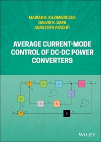
AVERAGE CURRENT-MODE CONTROL OF DC-DC POWER CONVERTERS An authoritative one-stop guide to the analysis, design, development, and control of a variety of power converter systems Average Current-Mode Control of DC-DC Power Converters provides comprehensive and up-to-date information about average current-mode control (ACMC) of pulse-width modulated (PWM) dc-dc converters. This invaluable one-stop resource covers both fundamental and state-of-the-art techniques in average current-mode control of power electronic converters???featuring novel small-signal models of non-isolated and isolated converter topologies with joint and disjoint switching elements and coverage of frequency and time domain analysis of controlled circuits. The authors employ a systematic theoretical framework supported by step-by-step derivations, design procedures for measuring transfer functions, challenging end-of-chapter problems, easy-to-follow diagrams and illustrations, numerous examples for different power supply specifications, and practical tips for developing power-stage small-signal models using circuit-averaging techniques. The text addresses all essential aspects of modeling, design, analysis, and simulation of average current-mode control of power converter topologies, such as buck, boost, buck-boost, and flyback converters in operating continuous-conduction mode (CCM). Bridging the gap between fundamental modeling methods and their application in a variety of switched-mode power supplies, this book: * Discusses the development of small-signal models and transfer functions related to the inner current and outer voltage loops * Analyzes inner current loops with average current-mode control and describes their dynamic characteristics * Presents dynamic properties of the poles and zeros, time-domain responses of the control circuits, and comparison of relevant modeling techniques * Contains a detailed chapter on the analysis and design of control circuits in time-domain and frequency-domain * Provides techniques required to produce professional MATLAB plots and schematics for circuit simulations, including example MATLAB codes for the complete design of PWM buck, boost, buck-boost, and flyback DC-DC converters * Includes appendices with design equations for steady-state operation in CCM for power converters, parameters of commonly used power MOSFETs and diodes, SPICE models of selected MOSFETs and diodes, simulation tools including introductions to SPICE, MATLAB, and SABER, and MATLAB codes for transfer functions and transient responses Average Current-Mode Control of DC-DC Power Converters is a must-have reference and guide for researchers, advanced graduate students, and instructors in the area of power electronics, and for practicing engineers and scientists specializing in advanced circuit modeling methods for various converters at different operating conditions.
Sie lesen das E-Book in den Legimi-Apps auf:
Seitenzahl: 309
Veröffentlichungsjahr: 2022
Ähnliche


Table of Contents
Cover
Title Page
Copyright
List of Symbols
About the Authors
Preface
Acknowledgments
1 Introduction
1.1 Principle of Operation of Conventional Average Current‐Mode Control Technique
1.2 Principle of Operation of Modified Average Current‐Mode Control Technique
1.3 Steady‐State Operation
2 Average Current‐Mode Control of Buck DC–DC Converter
2.1 Circuit Description, DC Characteristics, and Design
2.2 Large‐Signal and Small‐Signal Models of PWM Buck Converter in CCM
2.3 Power Stage Transfer Functions
2.4 Inner‐Current Loop
2.5 Closed‐Loop Transfer Functions for Inner‐Current Loop
2.6 Outer‐Voltage Loop
2.7 Closed‐Loop Transfer Functions for Outer‐Voltage Loop
2.8 Comparison of Closed‐Loop and Open‐Loop Step Responses
2.9 Summary
3 Average Current‐Mode Control of Boost DC–DC Converter
3.1 Circuit Description, DC Characteristics, and Design
3.2 Large‐Signal and Small‐Signal Models of PWM Boost Converter for CCM
3.3 Power‐Stage Transfer Functions
3.4 Inner‐Current Loop
3.5 Closed‐Loop Transfer Functions for Inner‐Current Loop
3.6 Outer‐Voltage Loop
3.7 Closed‐Loop Transfer Functions for Outer‐Voltage Loop
3.8 Comparison of Closed‐Loop and Open‐Loop Step Responses
3.9 Summary
4 Average Current‐Mode Control of Buck‐Boost DC–DC Converter
4.1 Circuit Description, DC Model, and Design
4.2 Large‐Signal and Small‐Signal Models of PWM Buck‐Boost Converter in CCM
4.3 Power‐Stage Transfer Functions
4.4 Inner‐Current Loop
4.5 Closed‐Inner Loop Transfer Functions
4.6 Outer‐Voltage Loop
4.7 Closed‐Loop Transfer Functions for Outer‐Voltage Loop
4.8 Comparison of Closed‐Loop and Open‐Loop Step Responses
4.9 Summary
5 Average Current‐Mode Control of Flyback DC–DC Converter
5.1 Circuit Description, DC Model, and Design
5.2 Large‐Signal and Small‐Signal Models of PWM Flyback Converter in CCM
5.3 Power‐Stage Transfer Functions
5.4 Inner‐Current Loop
5.5 Closed‐Loop Transfer Functions for Inner‐Current Loop
5.6 Outer‐Voltage Loop
5.7 Closed‐Loop Transfer Functions for Outer‐Voltage Loop
5.8 Comparison of Closed‐Loop and Open‐Loop Step Responses
5.9 Summary
References
Appendix A: Design Equations for Continuous‐Conduction Mode
A.1 Common Equations Needed for the Design of Converters
A.2 Specific Expressions for the Design of Converters in CCM
Appendix B: MOSFET Parameters
Appendix C: Diode Parameters
Appendix D: Selected MOSFETs' Spice Models
D.1 IRF430
D.2 IRF520
D.3 IRF150
D.4 IRF142
D.5 IRF840
D.6 IRF740
Appendix E: Selected Diodes' Spice Models
E.1 MUR1560
E.2 MBR10100
E.3 MBR1060
E.4 MUR2510
E.5 MBR2540
E.6 MBR4040
Appendix F: Simulation Tools
F.1 SPICE Model of Power MOSFETs
F.2 Introduction to SPICE
F.3 Introduction to
F.4 Introduction to SABER Circuit Simulator
Index
End User License Agreement
List of Tables
Chapter 2
Table 2.1 Summary of calculated values for open‐loop transfer functions.
Chapter 3
Table 3.1 Summary of calculated values for open‐loop transfer functions
Chapter 4
Table 4.1 Summary of calculated values for open‐loop transfer functions.
Chapter 5
Table 5.1 Summary of calculated values for the open‐loop transfer functions....
Appendix A: Design Equations for Continuous‐Conduction Mode
Table A.1 Steady‐state design equations for buck, boost, and buck–boost DC–D...
Appendix F: Simulation Tools
Table F.1 Selected SPICE level‐1 NMOS large‐signal model parameters.
List of Illustrations
Chapter 1
Figure 1.1 Boost DC–DC converter with a peak current‐mode control, showing o...
Figure 1.2 Circuit of a buck DC–DC converter with the conventional average c...
Figure 1.3 Waveforms showing the challenges encountered using conventional a...
Figure 1.4 Block diagram of the average current‐mode controlled DC–DC power ...
Figure 1.5 Circuit and key waveforms related to the feedback path in the ave...
Figure 1.6 Waveforms related to the average current‐mode controlled DC–DC bu...
Chapter 2
Figure 2.1 Circuit of the PWM buck converter.
Figure 2.2 Waveforms of the ideal switching network. (a) Gate‐to‐source volt...
Figure 2.3 DC model of PWM buck DC–DC converter in CCM.
Figure 2.4 Large‐signal nonlinear model of the PWM buck DC–DC converter in C...
Figure 2.5 Large‐signal linear model of the PWM buck DC–DC converter in CCM....
Figure 2.6 Small‐signal model of the PWM buck DC–DC converter in CCM.
Figure 2.7 Theoretically obtained plots of duty cycle‐to‐output voltage tran...
Figure 2.8 Theoretically obtained plots of duty cycle‐to‐inductor current tr...
Figure 2.9 Theoretically obtained plots of input‐to‐output voltage transfer ...
Figure 2.10 Theoretically obtained plots of input voltage‐to‐inductor curren...
Figure 2.11 Small‐signal model of the PWM buck DC–DC converter in CCM to der...
Figure 2.12 Theoretically obtained plots of output current‐to‐inductor curre...
Figure 2.13 Theoretically obtained plots of input impedance
. (a) Magnitude...
Figure 2.14 Theoretically obtained plots of output impedance
. (a) Magnitud...
Figure 2.15 Architecture of the inner‐current loop with low‐pass filter in t...
Figure 2.16 Circuit of the buck DC–DC converter with inner‐current loop.
Figure 2.17 Theoretically obtained plots of uncompensated loop gain
. (a) M...
Figure 2.18 Circuit of Type‐II controller.
Figure 2.19 Theoretically obtained plots of controller transfer function
. ...
Figure 2.20 Block diagram of inner‐current loop.
Figure 2.21 Theoretically obtained plots of compensated loop gain
of the i...
Figure 2.22 Block diagram used to derive the inner‐loop control‐to‐inductor ...
Figure 2.23 Theoretically obtained plots of inner‐current loop reference vol...
Figure 2.24 Block diagram required to derive the inner‐loop control‐to‐outpu...
Figure 2.25 Theoretically obtained plots of reference voltage‐to‐output volt...
Figure 2.26 Block diagram required to derive the inner‐loop input voltage‐to...
Figure 2.27 Theoretically obtained plots of input voltage‐to‐inductor curren...
Figure 2.28 Theoretically obtained plots of input voltage‐to‐output voltage ...
Figure 2.29 Block diagram used to derive the closed‐inner‐loop input impedan...
Figure 2.30 Theoretically obtained plots of closed‐inner‐loop input impedanc...
Figure 2.31 Block diagram required to derive the closed‐inner‐loop output im...
Figure 2.32 Theoretically obtained plots of closed‐inner‐loop output impedan...
Figure 2.33 Architecture of average current‐mode controlled buck converter w...
Figure 2.34 Circuit of the average current‐mode controlled buck converter wi...
Figure 2.35 Theoretically obtained plots of uncompensated loop gain
. (a) M...
Figure 2.36 Circuit of Type‐II controller used in outer‐voltage loop.
Figure 2.37 Theoretically obtained plots of controller transfer function
o...
Figure 2.38 Theoretically obtained plots of loop gain
of the compensated o...
Figure 2.39 Block diagram used to derive the control‐to‐output voltage trans...
Figure 2.40 Theoretically obtained plots of the reference voltage‐to‐output ...
Figure 2.41 Block diagram used to derive the input voltage to duty‐cycle tra...
Figure 2.42 Theoretically obtained plots of the input voltage‐to‐duty cycle ...
Figure 2.43 Block diagram used to derive the input voltage‐to‐output voltage...
Figure 2.44 Theoretically obtained plots of the input voltage‐to‐output volt...
Figure 2.45 Block diagram used to derive the closed‐outer‐voltage‐loop input...
Figure 2.46 Theoretically obtained plots of the closed‐outer‐voltage loop in...
Figure 2.47 Block diagram used to derive the closed‐outer‐voltage‐loop outpu...
Figure 2.48 Theoretically obtained plots of the closed‐outer‐voltage loop ou...
Figure 2.49 Comparison of responses in output voltage for step changes in in...
Figure 2.50 Comparison of responses in output voltage for step changes in du...
Figure 2.51 Comparison of responses in input current for step changes in the...
Figure 2.52 Comparison of responses in the output voltage for step changes i...
Chapter 3
Figure 3.1 Circuit of the PWM boost converter.
Figure 3.2 Key waveforms of the switching network. (a) Gate‐to‐source voltag...
Figure 3.3 DC model of PWM boost DC–DC converter.
Figure 3.4 Large‐signal nonlinear model of the PWM boost DC–DC converter in ...
Figure 3.5 Large‐signal linear model of the PWM boost DC–DC converter in CCM...
Figure 3.6 Small‐signal model of the PWM boost DC–DC converter in CCM.
Figure 3.7 Theoretically obtained plots of duty cycle‐to‐output voltage tran...
Figure 3.8 Response of the output voltage to step change in the duty cycle b...
Figure 3.9 Trajectory of the poles and zeros of
transfer function as funct...
Figure 3.10 Theoretically obtained plots of duty cycle‐to‐output voltage tra...
Figure 3.11 Trajectory of the poles and zeros of
transfer function as func...
Figure 3.12 The poles and zeros of
transfer function beyond the critical v...
Figure 3.13 Theoretically obtained plots of duty cycle‐to‐output voltage tra...
Figure 3.14 Theoretically obtained plots of duty cycle‐to‐inductor current t...
Figure 3.15 Response of the inductor current to step change in the duty cycl...
Figure 3.16 Trajectory of the poles and zeros of
transfer function as func...
Figure 3.17 Theoretically obtained plots of duty cycle‐to‐inductor current t...
Figure 3.18 Trajectory of the poles and zeros of
transfer function as func...
Figure 3.19 Theoretically obtained plots of duty cycle‐to‐inductor current t...
Figure 3.20 Theoretically obtained plots of input‐to‐output voltage transfer...
Figure 3.21 Theoretically obtained plots of input voltage‐to‐inductor curren...
Figure 3.22 Small‐signal model of the PWM boost DC–DC converter in CCM to de...
Figure 3.23 Theoretically obtained plots of output current‐to‐inductor curre...
Figure 3.24 Theoretically obtained plots of input impedance
. (a) Magnitude...
Figure 3.25 Theoretically obtained plots of output impedance
. (a) Magnit...
Figure 3.26 Architecture of the inner‐current loop with low‐pass ...
Figure 3.27 Circuit of the boost DC–DC converter with inner‐current loop.
Figure 3.28 Theoretically obtained plots of uncompensated loop gain
. (a)...
Figure 3.29 Circuit of Type‐II controller.
Figure 3.30 Theoretically obtained plots of controller transfer function
Figure 3.31 Theoretically obtained plots of compensated loop gain
of the...
Figure 3.32 Block diagram used to derive the inner‐loop control‐to‐inductor ...
Figure 3.33 Theoretically obtained plots of inner‐current loop reference vol...
Figure 3.34 Block diagram required to derive the inner‐loop control‐to‐outpu...
Figure 3.35 Theoretically obtained plots of reference voltage‐to‐output volt...
Figure 3.36 Block diagram required to derive the inner‐loop input voltage‐to...
Figure 3.37 Theoretically obtained plots of input voltage‐to‐inductor curren...
Figure 3.38 Block diagram required to derive the inner‐loop input voltage‐to...
Figure 3.39 Theoretically obtained magnitude and phase plots of input voltag...
Figure 3.40 Theoretically obtained plots of input voltage‐to‐duty cycle tran...
Figure 3.41 Block diagram used to derive the closed‐inner‐loop input impedan...
Figure 3.42 Theoretically obtained plots of closed‐inner‐loop input impedanc...
Figure 3.43 Block diagram required to derive the closed‐inner‐loop output im...
Figure 3.44 Theoretically obtained plots of closed‐inner‐loop output impedan...
Figure 3.45 Architecture of the average current‐mode controlled boost conver...
Figure 3.46 Circuit of the average current‐mode controlled boost converter w...
Figure 3.47 Theoretically obtained plots of uncompensated loop gain
. (a)...
Figure 3.48 Circuit of the Type‐II controller used in the outer‐voltage loop...
Figure 3.49 Theoretically obtained plots of controller transfer function
Figure 3.50 Theoretically obtained plots of loop gain
of the compensated...
Figure 3.51 Block diagram used to derive the control‐to‐output voltage trans...
Figure 3.52 Theoretically obtained plots of the reference voltage‐to‐output ...
Figure 3.53 Block diagram used to derive the input voltage‐to‐duty cycle tra...
Figure 3.54 Theoretically obtained plots of the input voltage‐to‐duty cycle ...
Figure 3.55 Block diagram used to derive the input voltage‐to‐output voltage...
Figure 3.56 Theoretically obtained plots of the input voltage‐to‐output volt...
Figure 3.57 Block diagram used to derive the closed‐outer‐voltage loop input...
Figure 3.58 Theoretically obtained plots of the closed‐outer‐voltage loop in...
Figure 3.59 Block diagram used to derive the closed‐outer‐voltage‐loop outpu...
Figure 3.60 Theoretically obtained plots of the closed‐outer‐voltage loop ou...
Figure 3.61 Comparison of responses in output voltage for step changes in in...
Figure 3.62 Comparison of responses in output voltage for step changes in du...
Figure 3.63 Comparison of responses in input current for step changes in the...
Figure 3.64 Comparison of responses in the output voltage for step changes i...
Chapter 4
Figure 4.1 Circuit of the PWM buck‐boost DC–DC converter.
Figure 4.2 Waveforms of ideal switching network. (a) Gate‐to‐source voltage ...
Figure 4.3 DC model of the PWM buck‐boost DC–DC converter in CCM.
Figure 4.4 Large‐signal nonlinear model of the PWM buck‐boost DC–DC converte...
Figure 4.5 Large‐signal linear model of the PWM buck‐boost DC–DC converter i...
Figure 4.6 Small‐signal model of the PWM buck‐boost DC–DC converter in CCM....
Figure 4.7 Small‐signal model of the PWM buck‐boost converter to derive the ...
Figure 4.8 Theoretically obtained plots of duty cycle‐to‐output voltage tran...
Figure 4.9 Trajectory of the poles and zeros of
transfer function as funct...
Figure 4.10 Theoretically obtained plots of duty cycle‐to‐output voltage tra...
Figure 4.11 Trajectory of the poles and zeros of
transfer function as func...
Figure 4.12 The poles and zeros of
transfer function beyond the critical v...
Figure 4.13 Theoretically obtained plots of duty cycle‐to‐output voltage tra...
Figure 4.14 Theoretically obtained plots of duty cycle‐to‐inductor current t...
Figure 4.15 Trajectory of the poles and zeros of
transfer function as func...
Figure 4.16 Theoretically obtained plots of duty cycle‐to‐inductor current t...
Figure 4.17 Trajectory of the poles and zeros of
transfer function as func...
Figure 4.18 Theoretically obtained plots of duty cycle‐to‐inducto...
Figure 4.19 Theoretically obtained plots of input‐to‐output voltage transfer...
Figure 4.20 Theoretically obtained plots of input voltage‐to‐inductor curren...
Figure 4.21 Small‐signal model of the PWM buck‐boost DC–DC converter in CCM ...
Figure 4.22 Theoretically obtained plots of output current‐to‐inductor curre...
Figure 4.23 Theoretically obtained plots of input impedance
. (a) Magnitude...
Figure 4.24 Theoretically obtained plots of output impedance
. (a) Magnitud...
Figure 4.25 Architecture of the inner‐current loop with low‐pass filter in t...
Figure 4.26 Circuit of the buck‐boost DC–DC converter with inner‐current loo...
Figure 4.27 Theoretically obtained plots of uncompensated loop gain
. (a) M...
Figure 4.28 Circuit of Type‐II controller used in inner‐current loop.
Figure 4.29 Theoretically obtained plots of controller transfer function
. ...
Figure 4.30 Block diagram of inner‐current loop.
Figure 4.31 Theoretically obtained plots of compensated loop gain
of the i...
Figure 4.32 Block diagram used to derive the inner‐loop control‐to‐inductor ...
Figure 4.33 Theoretically obtained plots of inner‐current loop reference vol...
Figure 4.34 Block diagram required to derive the inner‐loop control‐to‐outpu...
Figure 4.35 Theoretically obtained plots of reference voltage‐to‐output volt...
Figure 4.36 Block diagram required to derive the inner‐loop input voltage‐to...
Figure 4.37 Theoretically obtained plots of input voltage‐to‐inductor curren...
Figure 4.38 Block diagram required to derive the inner‐loop input voltage‐to...
Figure 4.39 Theoretically obtained plots of input voltage‐to‐output voltage ...
Figure 4.40 Theoretically obtained plots of input voltage‐to‐duty cycle tran...
Figure 4.41 Block diagram used to derive the inner‐closed loop input impeanc...
Figure 4.42 Theoretically obtained plots of closed‐inner‐loop input impedanc...
Figure 4.43 Block diagram required to derive the inner‐closed‐loop output im...
Figure 4.44 Theoretically obtained plots of closed‐inner‐loop output impedan...
Figure 4.45 Architecture of the complete average current‐mode controlled buc...
Figure 4.46 Complete circuit of the average current‐mode controlled buck‐boo...
Figure 4.47 Theoretically obtained plots of uncompensated loop gain
. (a) M...
Figure 4.48 Circuit of the Type‐II controller used in outer‐voltage loop.
Figure 4.49 Theoretically obtained plots of controller transfer function
o...
Figure 4.50 Theoretically obtained plots of loop gain
of the compensated o...
Figure 4.51 Block diagram used to derive the control‐to‐output voltage trans...
Figure 4.52 Theoretically obtained plots of the reference voltage‐to‐output ...
Figure 4.53 Block diagram used to derive the input voltage‐to‐duty cycle tra...
Figure 4.54 Theoretically obtained plots of the input voltage‐to‐duty cycle ...
Figure 4.55 Block diagram used to derive the input voltage‐to‐output voltage...
Figure 4.56 Theoretically obtained plots of the input voltage‐to‐output volt...
Figure 4.57 Block diagram used to derive the closed‐outer‐voltage‐loop input...
Figure 4.58 Theoretically obtained plots of the closed‐outer‐voltage loop in...
Figure 4.59 Block diagram used to derive the closed‐outer‐voltage‐loop outpu...
Figure 4.60 Theoretically obtained plots of the closed‐outer‐voltage loop ou...
Figure 4.61 Comparison of responses in output voltage for step changes in in...
Figure 4.62 Comparison of responses in output voltage for step changes in du...
Figure 4.63 Comparison of responses in input current for step changes in the...
Figure 4.64 Comparison of responses in the output voltage for step changes i...
Chapter 5
Figure 5.1 Circuit of the non‐inverting PWM flyback DC–DC converter.
Figure 5.2 Equivalent circuit of the non‐inverting PWM flyback DC–DC convert...
Figure 5.3 Waveforms of ideal switching network. (a) Gate‐to‐source voltage ...
Figure 5.4 DC model of the non‐inverting flyback DC–DC converter with resist...
Figure 5.5 DC model of the non‐inverting flyback DC–DC converter with equiva...
Figure 5.6 Large‐signal nonlinear model of the flyback DC–DC converter in CC...
Figure 5.7 Large‐signal linear model of the flyback DC–DC converter in CCM....
Figure 5.8 Small‐signal model of the flyback DC–DC converter in CCM.
Figure 5.9 Theoretically obtained plots of duty cycle‐to‐output voltage tran...
Figure 5.10 Trajectory of the poles and zeros of
transfer function as ...
Figure 5.11 Theoretically obtained plots of duty cycle‐to‐output voltage tra...
Figure 5.12 Trajectory of the poles and zeros of
transfer function as ...
Figure 5.13 Theoretically obtained plots of duty cycle‐to‐output voltage tra...
Figure 5.14 Trajectory of the poles and zeros of the
transfer function a...
Figure 5.15 The poles and zeros of
transfer function beyond the critical...
Figure 5.16 Theoretically obtained plots of duty cycle‐to‐output voltage tra...
Figure 5.17 Theoretically obtained plots of duty cycle‐to‐inductor current t...
Figure 5.18 Trajectory of the poles and zeros of
transfer function as a ...
Figure 5.19 Theoretically obtained plots of duty cycle‐to‐inductor current t...
Figure 5.20 Trajectory of the poles and zeros of the
transfer function a...
Figure 5.21 Theoretically obtained plots of duty cycle‐to‐inductor current t...
Figure 5.22 Trajectory of the poles and zeros of the
transfer function a...
Figure 5.23 Theoretically obtained plots of duty cycle‐to‐inductor current t...
Figure 5.24 Theoretically obtained plots of input‐to‐output voltage transfer...
Figure 5.25 Theoretically obtained plots of input voltage‐to‐inductor curren...
Figure 5.26 Small‐signal model of the PWM flyback DC–DC converter in CCM to ...
Figure 5.27 Theoretically obtained plots of output current‐to‐inductor curre...
Figure 5.28 Theoretically obtained plots of input impedance
. (a) Magnitu...
Figure 5.29 Theoretically obtained plots of output impedance
. (a) Magnit...
Figure 5.30 Architecture of the inner‐current loop with filter block.
Figure 5.31 Circuit of the flyback DC–DC converter with inner‐current loop....
Figure 5.32 Theoretically obtained plots of uncompensated loop gain
. (a)...
Figure 5.33 Circuit of the Type‐II controller.
Figure 5.34 Theoretically obtained plots of controller transfer function
Figure 5.35 Block diagram of the inner‐current loop.
Figure 5.36 Theoretically obtained plots of compensated loop gain
of the...
Figure 5.37 Block diagram used to derive the inner‐loop control‐to‐inductor ...
Figure 5.38 Theoretically obtained plots of inner‐current loop reference vol...
Figure 5.39 Block diagram required to derive the inner‐loop control‐to‐outpu...
Figure 5.40 Theoretically obtained plots of reference voltage‐to‐output volt...
Figure 5.41 Block diagram required to derive the inner‐loop input voltage‐to...
Figure 5.42 Theoretically obtained plots of input voltage‐to‐inductor curren...
Figure 5.43 Block diagram required to derive the inner‐loop input voltage‐to...
Figure 5.44 Theoretically obtained plots of input voltage‐to‐output voltage ...
Figure 5.45 Theoretically obtained plots of input voltage‐to‐duty cycle tran...
Figure 5.46 Block diagram used to derive the closed‐inner‐loop input impedan...
Figure 5.47 Theoretically obtained plots of closed‐inner‐loop input impedanc...
Figure 5.48 Block diagram required to derive the closed‐inner‐loop output im...
Figure 5.49 Theoretically obtained plots of closed‐inner‐loop output impedan...
Figure 5.50 Architecture of the complete average current‐mode controlled fly...
Figure 5.51 Complete circuit of the average current‐mode controlled flyback ...
Figure 5.52 Theoretically obtained plots of uncompensated loop gain
. (a)...
Figure 5.53 Circuit of Type‐II controller used in outer‐voltage loop.
Figure 5.54 Theoretically obtained plots of controller transfer function
Figure 5.55 Theoretically obtained plots of loop gain
of the compensated...
Figure 5.56 Block diagram used to derive the control‐to‐output voltage trans...
Figure 5.57 Theoretically obtained plots of the reference voltage‐to‐output ...
Figure 5.58 Block diagram used to derive the input voltage‐to‐duty cycle tra...
Figure 5.59 Theoretically obtained plots of the input voltage‐to‐duty cycle ...
Figure 5.60 Block diagram used to derive the input voltage‐to‐output voltage...
Figure 5.61 Theoretically obtained plots of the input voltage‐to‐output volt...
Figure 5.62 Block diagram used to derive the closed‐outer‐voltage‐loop input...
Figure 5.63 Theoretically obtained plots of the closed‐outer‐voltage loop in...
Figure 5.64 Block diagram used to derive the closed‐outer‐voltage‐loop outpu...
Figure 5.65 Theoretically obtained plots of the closed‐outer‐voltage loop ou...
Figure 5.66 Comparison of responses in output voltage for step changes in in...
Figure 5.67 Comparison of responses in output voltage for step changes in du...
Figure 5.68 Comparison of responses in input current for step changes in the...
Figure 5.69 Comparison of responses in the output voltage for step changes i...
Appendix F: Simulation Tools
Figure F.1 SPICE large‐signal model for
‐channel MOSFET.
Figure F.2 Theoretically obtained plots of duty cycle‐to‐output voltage tran...
Figure F.3 Step response for duty cycle‐to‐output voltage transfer function
Figure F.4 Poles and zeros of
transfer function as functions of the duty c...
Figure F.5 Theoretically obtained plots of duty cycle‐to‐inductor current tr...
Figure F.6 Step response for duty cycle‐to‐inductor current transfer functio...
Figure F.7 Trajectory of the poles and zeros of
transfer function as funct...
Figure F.8 Example circuit schematic in SABER.
Figure F.9 Example of plot window in SABER.
Guide
Cover
Title Page
Copyright
List of Symbols
About the Authors
Preface
Acknowledgments
Table of Contents
Begin Reading
References
Appendix A: Design Equations for Continuous‐Conduction Mode
Appendix B: MOSFET Parameters
Appendix C: Diode Parameters
Appendix D: Selected MOSFETs' Spice Models
Appendix E: Selected Diodes' Spice Models
Appendix F: Simulation Tools
Index
End User License Agreement
Pages
iii
vi
xiii
xiv
xv
xvi
xvii
xix
xx
xxi
1
2
3
4
5
6
7
8
9
10
11
12
13
14
15
16
17
18
19
20
21
22
23
24
25
26
27
28
29
30
31
32
33
34
35
36
37
38
39
40
41
42
43
44
45
46
47
48
49
50
51
52
53
54
55
56
57
58
59
61
62
63
64
65
66
67
68
69
70
71
72
73
74
75
76
77
78
79
80
81
82
83
84
85
86
87
88
89
90
91
92
93
94
95
96
97
98
99
100
101
102
103
104
105
106
107
108
109
110
111
112
113
114
115
116
117
118
119
120
121
122
123
124
125
126
127
128
129
130
131
132
133
134
135
136
137
138
139
140
141
142
143
144
145
146
147
148
149
150
151
152
153
154
155
156
157
158
159
160
161
162
163
164
165
166
167
168
169
170
171
172
173
174
175
176
177
178
179
180
181
182
183
184
185
186
187
188
189
190
191
192
193
194
195
196
197
198
199
200
201
202
203
204
205
206
207
208
209
210
211
212
213
214
215
216
217
218
219
220
221
222
223
224
225
226
227
228
229
230
231
232
233
234
235
236
237
238
239
240
241
242
243
244
245
246
247
248
249
250
251
252
253
254
255
256
257
258
259
260
261
262
263
264
265
266
267
269
270
271
272
273
275
276
277
279
281
282
283
284
285
286
287
288
289
290
291
292
293
294
295
296
297
298
299
300
301
302
303
305
306
307
308
309
310
Average Current-Mode Control of DC-DC Power Converters
Marian K. Kazimierczuk, Dalvir K. Saini, and Agasthya Ayachit
Department of Electrical Engineering, Wright State University, Dayton, Ohio, USA
This edition first published 2022
© 2022 John Wiley & Sons Ltd
All rights reserved. No part of this publication may be reproduced, stored in a retrieval system, or transmitted, in any form or by any means, electronic, mechanical, photocopying, recording or otherwise, except as permitted by law. Advice on how to obtain permission to reuse material from this title is available at http://www.wiley.com/go/permissions.
The right of Marian K. Kazimierczuk, Dalvir K. Saini, and Agasthya Ayachit to be identified as the authors of this work has been asserted in accordance with law.
Registered Offices
John Wiley & Sons, Inc., 111 River Street, Hoboken, NJ 07030, USA
John Wiley & Sons Ltd, The Atrium, Southern Gate, Chichester, West Sussex, PO19 8SQ, UK
Editorial Office
The Atrium, Southern Gate, Chichester, West Sussex, PO19 8SQ, UK
For details of our global editorial offices, customer services, and more information about Wiley products visit us at www.wiley.com.
Wiley also publishes its books in a variety of electronic formats and by print‐on‐demand. Some content that appears in standard print versions of this book may not be available in other formats.
Limit of Liability/Disclaimer of Warranty
While the publisher and authors have used their best efforts in preparing this work, they make no representations or warranties with respect to the accuracy or completeness of the contents of this work and specifically disclaim all warranties, including without limitation any implied warranties of merchantability or fitness for a particular purpose. No warranty may be created or extended by sales representatives, written sales materials or promotional statements for this work. The fact that an organization, website, or product is referred to in this work as a citation and/or potential source of further information does not mean that the publisher and authors endorse the information or services the organization, website, or product may provide or recommendations it may make. This work is sold with the understanding that the publisher is not engaged in rendering professional services. The advice and strategies contained herein may not be suitable for your situation. You should consult with a specialist where appropriate. Further, readers should be aware that websites listed in this work may have changed or disappeared between when this work was written and when it is read. Neither the publisher nor authors shall be liable for any loss of profit or any other commercial damages, including but not limited to special, incidental, consequential, or other damages.
Library of Congress Cataloging‐in‐Publication Data
Names: Kazimierczuk, Marian K., author. | Saini, Dalvir K., author. | Ayachit, Agasthya, author.
Title: Average current-mode control of DC-DC power converters / Marian K. Kazimierczuk, Dalvir K. Saini, and Agasthya Ayachit.
Description: Hoboken, NJ : Wiley, 2022. | Includes bibliographical references and index.
Identifiers: LCCN 2021039426 (print) | LCCN 2021039427 (ebook) | ISBN 9781119525653 (cloth) | ISBN 9781119525561 (adobe pdf) | ISBN 9781119525684 (epub)
Subjects: LCSH: Electric controllers. | DC-to-DC converters.
Classification: LCC TK2851 .K39 2022 (print) | LCC TK2851 (ebook) | DDC 621.31/32–dc23
LC record available at https://lccn.loc.gov/2021039426
LC ebook record available at https://lccn.loc.gov/2021039427
Cover Design: Wiley
Cover Image: © Image by Dalvir Saini
List of Symbols
A
i
load current‐to‐inductor current transfer function
A
io
DC gain of load current‐to‐inductor current transfer function
BW
bandwidth
C
filter capacitance
C
o
transistor output capacitance
D
DC component of on‐switch duty cycle
D
cr
critical duty cycle of switch
d
AC component of on‐switch duty cycle
d
T
large‐signal on‐switch duty cycle
f
c
gain crossover frequency
f
z
frequency of zero of transfer function
f
o
corner frequency or natural frequency
f
p
frequency of pole of transfer function
f
s
switching frequency
I
D
average or DC component of diode current
i
d
small‐signal AC component of diode current
i
D
large‐signal diode current
I
I
average or DC component of input current
i
i
small‐signal AC component of input current
i
I
large‐signal component of input current
I
L
average or DC component of inductor current
i
l
small‐signal AC component of inductor current
i
L
large‐signal inductor current
I
O
DC component of load current
i
o
small‐signal AC component of load current
i
O
large‐signal load current
I
S
DC component of switch current
i
s
small‐signal AC component of switch current
i
S
large‐signal switch current
i
C
large‐signal filter capacitor current
L
inductor or inductance
M
di
input voltage to duty‐cycle transfer function relevant to inner‐current loop
M
dv
input voltage to duty‐cycle transfer function relevant to outer‐voltage loop
M
MID
DC current transfer function of converter
M
Mic
input voltage‐to‐inductor current transfer function
M
v
open‐loop input‐to‐output voltage transfer function
M
MVD
DC voltage transfer function of a converter
M
Mvc
input‐to‐output voltage transfer function relevant to outer‐voltage loop
M
vi
open‐loop input voltage‐to‐inductor current transfer function
M
Mvic
input‐to‐output voltage transfer function relevant to inner‐current loop
M
Mvi
open‐loop input voltage‐to‐inductor current transfer function at DC
M
vo
open‐loop input‐to‐output voltage function at DC
PM
phase margin
P
I
converter DC input power
P
LS
converter power loss
P
O
converter DC output power
P
RF
conduction loss in diode forward resistance
R
F
P
rC
conduction loss in equivalent series resistance of the filter capacitor
P
VF
conduction loss in diode forward voltage
V
F
r
equivalent averaged resistance
R
Riic
real component of input impedance relevant to inner‐current loop
R
Roic
real component of output impedance relevant to inner‐current loop
R
Rivc
real component of input impedance relevant to outer‐voltage loop
R
Rovc
real component of output impedance relevant to outer‐voltage loop
R
F
diode forward resistance
R
L
load resistance
r
C
equivalent series resistance (ESR) of filter capacitor
r
L
equivalent series resistance (ESR) of inductor
r
DS
ON
resistance of switch
R
s
sense resistance
T
switching period, Loop gain
T
ci
voltage transfer function of controller relevant to inner‐current loop
T
cv
voltage transfer function of controller relevant to outer‐voltage loop
T
f
low‐pass filter transfer function
T
i
loop gain of inner‐current loop
T
v
loop gain of outer‐voltage loop in the presence of inner‐current loop
T
ki
uncompensated loop gain of inner‐current loop
T
kv
uncompensated loop gain of outer‐voltage loop in the presence of inner‐current loop
T
m
transfer function of pulse‐width modulator
T
p
open‐loop duty cycle‐to‐output transfer function
T
pi
open‐loop duty cycle‐to‐inductor current transfer function
T
po
open‐loop control‐to‐output transfer function at DC
T
Tpi
open‐loop control‐to‐inductor current transfer function at DC
T
Tic
reference voltage‐to‐inductor current transfer function
T
Tpc
reference voltage‐to‐output voltage transfer function relevant to outer‐voltage loop
T
Tpic
reference voltage‐to‐output voltage transfer function relevant to inner‐current loop
T
v
loop gain of outer‐voltage loop
V
C
DC component of control voltage
v
C
total control voltage
v
c
AC component of control voltage
V
CI
DC component of control voltage relevant to inner‐current loop
V
VCp
peak‐to‐peak ripple voltage of the filter capacitor
V
D
DC component of diode voltage
v
D
large‐signal component of diode voltage
V
EI
DC component of error voltage relevant to inner‐current loop
v
EI
total error voltage relevant to inner‐current loop
v
ei
AC component of error voltage relevant to inner‐current loop
V
EV
DC component of error voltage relevant to outer‐voltage loop
v
ev
AC component of error voltage relevant to outer‐voltage loop
v
EV
total error voltage relevant to outer‐voltage loop
V
F
diode forward voltage
V
FI
DC component of feedback voltage relevant to inner‐current loop
v
FI
total feedback voltage relevant to inner‐current loop
v
fi
AC component of feedback voltage relevant to inner‐current loop
V
FV
DC component of feedback voltage relevant to outer‐voltage loop
v
FV
total feedback voltage relevant to outer‐voltage loop
v
fv
AC component of feedback voltage relevant to outer‐voltage loop
V
I
DC component of input voltage
v
i
small‐signal AC component of input voltage
v
I
large‐signal component of input voltage
V
O
DC component of output voltage
v
o
AC component of output voltage
v
O
large‐signal component of output voltage
V
RI
reference voltage relevant to inner‐current loop
v
ri
AC component of reference voltage relevant to inner‐current loop
V
RS
DC voltage across sense resistor
V
RV
reference voltage relevant to outer‐voltage loop
v
rv
AC component of reference voltage relevant to outer‐voltage loop
v
rc
voltage across ESR of filter capacitor
V
r
peak‐to‐peak value of ripple component of the output voltage
V
Tm
peak ramp voltage of pulse‐width modulator
v
L
voltage across inductor
X
Xiic
imaginary component of input impedance relevant to inner‐current loop
X
Xoic
imaginary component of output impedance relevant to inner‐current loop
X
Xivc
imaginary component of input impedance relevant to outer‐voltage loop
X
Xovc
imaginary component of output impedance relevant to outer‐voltage loop
Z
i
open‐loop input impedance
Z
io
open‐loop input impedance at DC (
R
i
)
Z
Ziic
input impedance relevant to inner‐current loop
Z
Zivc
input impedance relevant to outer‐voltage loop
Z
o
open‐loop output impedance
Z
oo
open‐loop output impedance at DC (
R
o
)
Z
Zoic
closed‐loop output impedance relevant to inner‐current loop
Z
Zovc
closed‐loop output impedance relevant to outer‐voltage current
β
transfer function of feedback network
η
efficiency of converter
ξ
damping ratio
σ
real component of complex‐conjugate poles
ω
angular frequency
ω
unity‐gain angular crossover frequency
ω
o
corner frequency or angular frequency
ω
p
angular frequency of simple pole
ω
z
angular frequency of simple zero


