132,99 €
Mehr erfahren.
- Herausgeber: John Wiley & Sons
- Kategorie: Wissenschaft und neue Technologien
- Serie: IEEE Press Series on Microelectronic Systems
- Sprache: Englisch
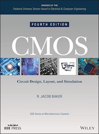
A revised guide to the theory and implementation of CMOS analog and digital IC design
The fourth edition of CMOS: Circuit Design, Layout, and Simulation is an updated guide to the practical design of both analog and digital integrated circuits. The author—a noted expert on the topic—offers a contemporary review of a wide range of analog/digital circuit blocks including: phase-locked-loops, delta-sigma sensing circuits, voltage/current references, op-amps, the design of data converters, and switching power supplies.
CMOS includes discussions that detail the trade-offs and considerations when designing at the transistor-level. The companion website contains numerous examples for many computer-aided design (CAD) tools. Using the website enables readers to recreate, modify, or simulate the design examples presented throughout the book. In addition, the author includes hundreds of end-of-chapter problems to enhance understanding of the content presented. This newly revised edition:
• Provides in-depth coverage of both analog and digital transistor-level design techniques
• Discusses the design of phase- and delay-locked loops, mixed-signal circuits, data converters, and circuit noise
• Explores real-world process parameters, design rules, and layout examples
• Contains a new chapter on Power Electronics
Written for students in electrical and computer engineering and professionals in the field, the fourth edition of CMOS: Circuit Design, Layout, and Simulation is a practical guide to understanding analog and digital transistor-level design theory and techniques.
Sie lesen das E-Book in den Legimi-Apps auf:
Seitenzahl: 1918
Veröffentlichungsjahr: 2019
Ähnliche
IEEE Press
445 Hoes LanePiscataway, NJ 08854
IEEE Press Editorial Board
Ekram Hossain,
Editor in Chief
Giancarlo FortinoDavid Alan GrierDonald HeirmanXiaoou Li
Andreas MolischSaeid NahavandiRay PerezJeffrey Reed
Diomidis SpinellisElya B. JoffeSarah SpurgeonAhmet Murat Tekalp
CMOS Circuit Design,Layout, and Simulation
Fourth Edition
R. Jacob Baker
IEEE Press Series on Microelectronic Systems
Copyright © 2019 by The Institute of Electrical and Electronics Engineers, Inc. All rights reserved.
Published by John Wiley & Sons, Inc., Hoboken, New Jersey. Published simultaneously in Canada.
No part of this publication may be reproduced, stored in a retrieval system, or transmitted in any form or by any means, electronic, mechanical, photocopying, recording, scanning, or otherwise, except as permitted under Section 107 or 108 of the 1976 United States Copyright Act, without either the prior written permission of the Publisher, or authorization through payment of the appropriate per-copy fee to the Copyright Clearance Center, Inc., 222 Rosewood Drive, Danvers, MA 01923, (978) 750-8400, fax (978) 750-4470, or on the web at www.copyright.com. Requests to the Publisher for permission should be addressed to the Permissions Department, John Wiley & Sons, Inc., 111 River Street, Hoboken, NJ 07030, (201) 748-6011, fax (201) 748-6008, or online at http://www.wiley.com/go/permission.
Limit of Liability/Disclaimer of Warranty: While the publisher and author have used their best efforts in preparing this book, they make no representations or warranties with respect to the accuracy or completeness of the contents of this book and specifically disclaim any implied warranties of merchantability or fitness for a particular purpose. No warranty may be created or extended by sales representatives or written sales materials. The advice and strategies contained herein may not be suitable for your situation. You should consult with a professional where appropriate. Neither the publisher nor author shall be liable for any loss of profit or any other commercial damages, including but not limited to special, incidental, consequential, or other damages.
For general information on our other products and services or for technical support, please contact our Customer Care Department within the United States at (800) 762-2974, outside the United States at (317) 572-3993 or fax (317) 572-4002.
Wiley also publishes its books in a variety of electronic formats. Some content that appears in print may not be available in electronic formats. For more information about Wiley products, visit our web site at www.wiley.com.
Library of Congress Cataloging-in-Publication Data is available.
ISBN 9781119481515
To Julie
CONTENTS
Cover
Preface
Chapter 1 Introduction to CMOS Design
1.1 The CMOS IC Design Process
1.2 CMOS Background
1.3 An Introduction to SPICE
Chapter 2 The Well
2.1 Patterning
2.2 Laying Out the N-well
2.3 Resistance Calculation
2.4 The N-well/Substrate Diode
2.5 The RC Delay through an N-well
2.6 Twin Well Processes
Chapter 3 The Metal Layers
3.1 The Bonding Pad
3.2 Design and Layout Using the Metal Layers
3.3 Crosstalk and Ground Bounce
3.4 Layout Examples
Note
Chapter 4 The Active and Poly Layers
4.1 Layout using the Active and Poly Layers
4.2 Connecting Wires to Poly and Active
4.3 Electrostatic Discharge (ESD) Protection
Chapter 5 Resistors, Capacitors, MOSFETs
5.1 Resistors
5.2 Capacitors
5.3 MOSFETs
5.4 Layout Examples
Chapter 6 MOSFET Operation
6.1 MOSFET Capacitance Overview/Review
6.2 The Threshold Voltage
6.3 IV Characteristics of MOSFETs
6.4 SPICE Modeling of the MOSFET
6.5 Short-Channel MOSFETs
Note
Chapter 7 CMOS Fabrication
7.1 CMOS Unit Processes
7.2 CMOS Process Integration
7.3 Backend Processes
7.4 Advanced CMOS Process Integration
7.5 Summary
Notes
Chapter 8 Electrical Noise: An Overview
8.1 Signals
8.2 Circuit Noise
8.3 Discussion
Note
Chapter 9 Models for Analog Design
9.1 Long-Channel MOSFETs
9.2 Short-Channel MOSFETs
9.3 MOSFET Noise Modeling
Chapter 10 Models for Digital Design
10.1 The Digital MOSFET Model
10.2 The MOSFET Pass Gate
10.3 A Final Comment Concerning Measurements
Chapter 11 The Inverter
11.1 DC Characteristics
11.2 Switching Characteristics
11.3 Layout of the Inverter
11.4 Sizing for Large Capacitive Loads
11.5 Other Inverter Configurations
Chapter 12 Static Logic Gates
12.1 DC Characteristics of the NAND and NOR Gates
12.2 Layout of the NAND and NOR Gates
12.3 Switching Characteristics
12.4 Complex CMOS Logic Gates
Chapter 13 Clocked Circuits
13.1 The CMOS TG
13.2 Applications of the Transmission Gate
13.3 Latches and Flip-Flops
13.4 Examples
Chapter 14 Dynamic Logic Gates
14.1 Fundamentals of Dynamic Logic
14.2 Clocked CMOS Logic
Chapter 15 CMOS Layout Examples
15.1 Chip Layout
15.2 Layout Steps
by Dean Moriarty
Note
Chapter 16 Memory Circuits
16.1 Array Architectures
16.2 Peripheral Circuits
16.3 Memory Cells
Chapter 17 Sensing Using ΔΣ Modulation
17.1 Qualitative Discussion
17.2 Sensing Resistive Memory
17.3 Sensing in CMOS Imagers
Chapter 18 Special Purpose CMOS Circuits
18.1 The Schmitt Trigger
18.2 Multivibrator Circuits
18.3 Input Buffers
18.4 Charge Pumps (Voltage Generators)
Chapter 19 Digital Phase-Locked Loops
19.1 The Phase Detector
19.2 The Voltage-Controlled Oscillator
19.3 The Loop Filter
19.4 System Considerations
19.5 Delay-Locked Loops
19.6 Some Examples
Note
Chapter 20 Current Mirrors
20.1 The Basic Current Mirror
20.2 Cascoding the Current Mirror
20.3 Biasing Circuits
Chapter 21 Amplifiers
21.1 Gate-Drain-Connected Loads
21.2 Current Source Loads
21.3 The Push-Pull Amplifier
Chapter 22 Differential Amplifiers
22.1 The Source-Coupled Pair
22.2 The Source Cross-Coupled Pair
22.3 Cascode Loads (The Telescopic Diff-Amp)
22.4 Wide-Swing Differential Amplifiers
Chapter 23 Voltage References
23.1 MOSFET-Resistor Voltage References
23.2 Parasitic Diode-Based References
Chapter 24 Operational Amplifiers I
24.1 The Two-Stage Op-Amp
24.2 An Op-Amp with Output Buffer
24.3 The Operational Transconductance Amplifier (OTA)
24.4 Gain-Enhancement
24.5 Some Examples and Discussions
Chapter 25 Dynamic Analog Circuits
25.1 The MOSFET Switch
25.2 Fully-Differential Circuits
25.3 Switched-Capacitor Circuits
25.4 Circuits
Chapter 26 Operational Amplifiers II
26.1 Biasing for Power and Speed
26.2 Basic Concepts
26.3 Basic Op-Amp Design
26.4 Op-Amp Design Using Switched-Capacitor CMFB
Chapter 27 Nonlinear Analog Circuits
27.1 Basic CMOS Comparator Design
27.2 Adaptive Biasing
27.3 Analog Multipliers
Chapter 28 Data Converter Fundamentals
28.1 Analog Versus Discrete Time Signals
28.2 Converting Analog Signals to Digital Signals
28.3 Sample-and-Hold (S/H) Characteristics
28.4 Digital-to-Analog Converter (DAC) Specifications
28.5 Analog-to-Digital Converter (ADC) Specifications
28.6 Mixed-Signal Layout Issues
Chapter 29 Data Converter Architectures
29.1 DAC Architectures
29.2 ADC Architectures
Chapter 30 Implementing Data Converters
30.1
R-2R
Topologies for DACs
30.2 Op-Amps in Data Converters
30.3 Implementing ADCs
Chapter 31 Feedback Amplifiers
31.1 The Feedback Equation
31.2 Properties of Negative Feedback on Amplifier Design
31.3 Recognizing Feedback Topologies
31.4 The Voltage Amp (Series-Shunt Feedback)
31.5 The Transimpedance Amp (Shunt-Shunt Feedback)
31.6 The Transconductance Amp (Series-Series Feedback)
31.7 The Current Amplifier (Shunt-Series Feedback)
31.8 Stability
31.9 Design Examples
Note
Chapter 32 Hysteretic Power Converters
32.1 A Review of Power and Energy Basics
32.2 Switching Power Supplies: Some Examples
32.3 Hysteretic Control
Note
Index
About the Author
END USER LICENSE AGREEMENT
List of Tables
Chapter 2
Table 2.1
Chapter 3
Table 3.1
Table 3.2
Chapter 4
Table 4.1
Chapter 5
Table 5.1
Chapter 6
Table 6.1
Table 6.2
Table 6.3
Table 6.4
Chapter 7
Table 7.1
Chapter 8
Table 8.1
Table 8.2
Chapter 9
Table 9.1
Table 9.2
Chapter 10
Table 10.1
Table 10.2
Chapter 16
Table 16.1
Chapter 17
Table 17.1
Table 17.2
Table 17.3
Chapter 20
Table 20.1
Chapter 29
Table 29.1
Chapter 30
Table 30.1
Chapter 31
Table 31.1
Table 31.2


