120,99 €
Mehr erfahren.
- Herausgeber: Wiley-VCH Verlag GmbH & Co. KGaA
- Kategorie: Wissenschaft und neue Technologien
- Sprache: Englisch
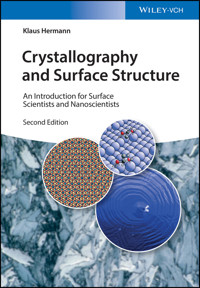
A valuable learning tool as well as a reference, this book provides students and researchers in surface science and nanoscience with the theoretical crystallographic foundations, which are necessary to understand local structure and symmetry of bulk crystals, including ideal and real single crystal surfaces. The author deals with the subject at an introductory level, providing numerous graphic examples to illustrate the mathematical formalism. The book brings together and logically connects many seemingly disparate structural issues and notations used frequently by surface scientists and nanoscientists. Numerous exercises of varying difficulty, ranging from simple questions to small research projects, are included to stimulate discussions about the different subjects.
From the contents:
Bulk Crystals, Three-Dimensional Lattices
- Crystal Layers, Two-Dimensional Lattices, Symmetry
- Ideal Single Crystal Surfaces
- Real Crystal Surfaces
- Adsorbate layers
- Interference Lattices
- Chiral Surfaces
- Experimental Analysis of Real Crystal Surfaces
- Nanoparticles and Crystallites
- Quasicrystals
- Nanotubes
Sie lesen das E-Book in den Legimi-Apps auf:
Seitenzahl: 704
Veröffentlichungsjahr: 2016
Ähnliche


Table of Contents
Cover
Title Page
Copyright
Preface to the Second Edition
Preface to the First Edition
Chapter 1: Introduction
Chapter 2: Bulk Crystals: Three-Dimensional Lattices
2.1 Basic Definition
2.2 Representation of Bulk Crystals
2.3 Periodicity Cells of Lattices
2.4 Lattice Symmetry
2.5 Reciprocal Lattice
2.6 Neighbor Shells
2.7 Nanoparticles and Crystallites
2.8 Incommensurate Crystals and Quasicrystals
2.9 Exercises
Chapter 3: Crystal Layers: Two-Dimensional Lattices
3.1 Basic Definition, Miller Indices
3.2 Netplane-Adapted Lattice Vectors
3.3 Symmetrically Appropriate Lattice Vectors: Minkowski Reduction
3.4 Miller Indices for Cubic and Trigonal Lattices
3.5
Alternative Definition of Miller Indices and Miller
–
Bravais Indices
3.6 Symmetry Properties of Netplanes
3.7 Crystal Systems and Bravais Lattices in Two Dimensions
3.8 Crystallographic Classification of Netplanes and Monolayers
3.9 Exercises
Chapter 4: Ideal Single Crystal Surfaces
4.1 Basic Definition, Termination
4.2 Morphology of Surfaces, Stepped and Kinked Surfaces
4.3 Miller Index Decomposition
4.4 Chiral and Achiral Surfaces
4.5 Exercises
Chapter 5: Real Crystal Surfaces
5.1 Surface Relaxation
5.2 Surface Reconstruction
5.3 Growth Processes
5.4 Faceting
5.5 Exercises
Chapter 6: Adsorbate Layers
6.1 Definition and Classification
6.2 Adsorbate Sites
6.3 Wood Notation of Surface Structure
6.4 High-Order Commensurate (HOC) Overlayers
6.5 Interference Lattices
6.6 Symmetry and Domain Formation
6.7 Adsorption at Surfaces and Chirality
6.8 Exercises
Chapter 7: Experimental Analysis of Real Crystal Surfaces
7.1 Experimental Methods
7.2 Surface Structure Compilations
7.3 Database Formats for Surface and Nanostructures
7.4 Exercises
Chapter 8: Nanotubes
8.1 Basic Definition
8.2 Nanotubes and Symmetry
8.3 Complex Nanotubes
8.4 Exercises
Appendix A: Sketches of High-Symmetry Adsorbate Sites
A.1 Face-Centered Cubic (fcc) Surface Sites
A.2 Body-Centered Cubic (bcc) Surface Sites
A.3 Hexagonal Close-Packed (hcp) Surface Sites
A.4 Diamond Surface Sites
A.5 Zincblende Surface Sites
Appendix B: Parameter Tables of Crystals
Appendix C: Mathematics of the Wood Notation
3.1 Basic Formalism and Examples
3.2 Wood-Representability
Appendix D: Mathematics of the Minkowski Reduction
Appendix E: Details of Number Theory
E.1 Basic Definitions and Functions
E.2 Euclid's Algorithm
E.3 Linear Diophantine Equations
E.4 Quadratic Diophantine Equations
E.5 Number Theory and 2 × 2 Matrices
Appendix F: Details of Vector Calculus and Linear Algebra
Appendix G: Details of Fourier Theory
Appendix H: List of Surface Web Sites
Appendix I: List of Surface Structures
Glossary and Abbreviations
References
Index
End User License Agreement
Pages
ix
x
xi
xii
1
2
3
4
5
7
8
9
10
11
12
13
14
15
16
17
18
19
20
21
22
23
24
25
26
27
28
29
30
31
32
33
34
35
36
37
38
39
40
41
42
43
44
45
46
47
48
49
50
51
52
53
54
55
56
57
58
59
60
61
62
63
64
65
66
67
68
69
70
71
72
73
74
75
76
77
78
79
80
81
82
83
84
85
86
87
88
89
91
92
93
94
95
96
97
98
99
100
101
102
103
104
105
106
107
108
109
110
111
112
113
114
115
116
117
118
119
120
121
122
123
124
125
126
127
128
129
130
131
132
133
134
135
136
137
138
139
140
141
142
143
144
145
146
147
148
149
150
151
152
153
154
155
156
157
158
159
160
161
162
163
164
165
166
167
168
169
170
171
172
173
174
175
176
177
178
179
180
181
182
183
184
185
186
187
188
189
190
191
192
193
194
195
196
197
198
199
200
201
202
203
204
205
206
207
209
210
211
212
213
214
215
216
217
218
219
220
221
222
223
224
225
226
227
228
229
230
231
232
233
235
236
237
238
239
240
241
242
243
244
245
246
247
248
249
250
251
252
253
254
255
256
257
258
259
260
261
262
263
264
265
266
267
268
269
270
271
272
273
274
275
276
277
278
279
280
281
282
283
284
285
286
287
288
289
290
291
292
293
294
295
296
297
298
299
300
301
302
303
304
305
306
307
308
309
310
311
312
313
314
315
316
317
318
319
320
321
322
323
324
325
326
327
329
330
331
332
333
334
335
336
337
338
339
340
341
342
343
344
345
346
347
348
351
355
356
357
358
359
360
361
362
363
364
365
367
368
369
370
371
372
373
374
375
376
377
378
379
380
381
382
383
384
385
386
387
388
389
391
392
393
394
395
396
397
399
401
402
403
404
405
406
407
408
409
410
411
412
413
414
415
416
417
418
419
420
421
422
423
425
426
427
428
429
430
431
432
Guide
Cover
Table of Contents
Preface to the Second Edition
Begin Reading
List of Illustrations
Chapter 1: Introduction
Figure 1.1 Section of an MgO crystal (NaCl lattice). The atoms are shown as shaded balls of different color and labeled accordingly. The section is enclosed by nonpolar (0 0 1), (−1 1 0), and by polar (1 1 1) oriented surfaces.
Chapter 2: Bulk Crystals: Three-Dimensional Lattices
Figure 2.1 Section of a tetragonal YBa
2
Cu
3
O
7
crystal. The atoms are labeled accordingly. In addition, the basis of 13 atoms inside a rectangular cell and lattice vectors , , are included to the left.
Figure 2.2 (a) Section of a cubic CsCl crystal. Sticks connect neighboring Cs atoms to indicate the crystal structure. (b) Primitive morphological unit cell with two atoms, Cs and Cl, inside. The lattice vectors , , as well as lattice basis vectors, = 0 for Cs and for Cl, are shown and labeled accordingly.
Figure 2.3 Definition of crystallographic lattice parameters
a, b
,
c
, α, β, γ in a perspective view.
Figure 2.4 Decomposition of the YBa
2
Cu
3
O
7
crystal (a) into its copper oxide, Cu
3
O
7
(b) and heavy metal, YBa
2
, components (c). Atoms are shown as colored balls and labeled accordingly. In addition, the lattice vectors , , are indicated by arrows.
Figure 2.5 Decomposition of the diamond crystal into two (shifted) face-centered cubic crystals, denoted fcc
1
(gray balls, black lines) and fcc
2
(red balls and red lines). The crystal is shown in a stereo view where the visual three-dimensional impression is obtained by cross-eyed viewing.
Figure 2.6 Lattice vectors , , of the body-centered cubic (bcc) lattice sketched inside a cubic frame with Cartesian coordinates, x, y, and z, indicated. Atoms of the corresponding bcc crystal are shown as balls.
Figure 2.7 Visual decomposition of the bcc crystal into two (shifted) sc crystals, denoted sc
1
(gray balls, black lines) and sc
2
(red balls and lines). The crystal is shown in a stereo view where the visual three-dimensional impression is obtained by cross-eyed viewing.
Figure 2.8 Lattice vectors , , of the fcc lattice sketched inside a cubic frame and labeled accordingly. Atoms of the corresponding fcc crystal are shown as balls. The dashed lines are meant to assist the visual orientation inside the figure.
Figure 2.9 Visual decomposition of the fcc crystal into four (shifted) sc crystals, denoted sc
1
(dark gray balls, black lines), sc
2
(dark red balls and lines), sc
3
(light gray balls and lines), and sc
4
(light red balls and lines). The crystal is shown in a stereo view where the visual three-dimensional impression is obtained by cross-eyed viewing.
Figure 2.10 (a) Section of a hexagonal crystal with close-packed geometry (hcp). Sticks connect atoms with nearest and second nearest neighbors to indicate the crystal structure. (b) Primitive morphological unit cell with two atoms inside. The lattice vectors , , (obtuse representation) are labeled accordingly. The unit cell is embedded in a hexagonal environment (dashed lines) to indicate its symmetry.
Figure 2.11 (a) Lattice vectors , , of the trigonal (rhombohedral) lattice with definitions of the Cartesian coordinate system and of angles ϕ, α, see text. (b) Three trigonal lattices combining to form a non-primitive hexagonal lattice. Lattice vectors are shown by arrows, black for trigonal and red for hexagonal. The visual correlation between the two lattices is indicated by thin gray sticks connecting hexagonal lattice points.
Figure 2.12 Fictitious sc crystal with ferromagnetic (left) and anti-ferromagnetic ordering (right). Atoms are shown as dark (spin up) and light (spin down) balls with their spin orientation indicated by black and red arrows. The superlattice vectors , , and primitive lattice vectors , , are labeled accordingly.
Figure 2.13 Structure of MgO substrate confined by (1 0 0) and (−1 0 0) oriented surfaces in repeated slab geometry (three slabs). The superlattice vectors ,
2,
are labeled accordingly.
Figure 2.14 Structure of silver substrate confined by (12 11 7) and (−12 −11 −7) oriented surfaces in repeated slab geometry (three slabs). The superlattice vectors ,
2,
are labeled accordingly.
Figure 2.15 Alternative description of the square lattice by lattice vectors , and , , respectively. The morphological unit cells of the two descriptions are emphasized by gray painting.
Figure 2.16 (a) Section of a bcc iron (Fe) crystal. Sticks between atom balls indicate the crystal structure. (b) Non-primitive sc morphological unit cell with two iron atoms inside. Lattice vectors , , , and ′ are labeled accordingly.
Figure 2.17 Non-primitive morphological unit cell with choices (a–d) for possible lattice vectors inside the cell. The possible lattice vectors , , , , as well as the lattice vectors , , defining the morphological unit cell are labeled accordingly. The dashed lines are meant to assist the visual orientation inside the figure.
Figure 2.18 Different centering of morphological unit cells. (a) Primitive, (b) I-centered, (c) A-centered, (d) B-centered, (e) C-centered, and (f) F-centered cell. The lattice vectors , , defining the morphological unit cell are labeled accordingly. The dashed lines are meant to assist the visual orientation inside the cells.
Figure 2.19 Alternative unit cells of the square lattice. The different unit cells are emphasized by red filling. The lattice vectors and are sketched at lower left corner.
Figure 2.20 (a) Morphological unit cell (Niggli cell) and (b) Wigner–Seitz cell of the bcc lattice. The polygonal cells are shaded in gray with lattice vectors labeled accordingly. The dashed lines are meant to assist the visual orientation inside the figures.
Figure 2.21 (a) Morphological unit cell (Niggli cell) and (b) Wigner–Seitz cell of the fcc lattice. The polygonal cells are shaded in gray with lattice vectors labeled accordingly. The dashed lines are meant to assist the visual orientation inside the figures.
Figure 2.22 Shape of Wigner–Seitz cells of the centered tetragonal (ct) lattice for different ratios q =
c
/
a
. Here q = 1 and q = represent the bcc and fcc lattice, respectively. The top Figure refer to rectangular blocks of a fictitious monoatomic ct crystal illustrating the lattice structure for corresponding ratios q.
Figure 2.23 Morphological unit cell of the triclinic-P lattice with lattice vectors , , and angles α, β, γ labeled accordingly.
Figure 2.24 Morphological unit cells of the monoclinic crystal system, (a) monoclinic-P and (b) monoclinic-B lattices with lattice vectors , , and angles α = β = 90°, γ labeled accordingly (angles only for monoclinic-P). Angles of 90° are indicated by small rectangles filled with a dot. The dashed line connecting opposing lattice points is meant to guide the eye.
Figure 2.25 Morphological unit cells of the orthorhombic crystal system, (a) orthorhombic-P, (b) orthorhombic-C, (c) orthorhombic-I, and (d) orthorhombic-F, lattices with lattice vectors , , and angles α = β = γ = 90° labeled accordingly (angles only for orthorhombic-P indicated by small rectangles filled with a dot). The dashed lines connecting lattice points are meant to guide the eye.
Figure 2.26 Morphological unit cells of the tetragonal crystal system, (a) tetragonal-P and (b) tetragonal-I lattices with lattice vectors , , and angles α = β = γ = 90° labeled accordingly (angles only for tetragonal-P indicated by small rectangles filled with a dot). Parallel pairs of short lines indicate vectors of equal length. The dashed line connecting opposing lattice points is meant to guide the eye.
Figure 2.27 Morphological unit cells of the cubic crystal system, (a) cubic-P, (b) cubic-I, and (c) cubic-F, lattices with lattice vectors , , and angles α = β = γ = 90° labeled accordingly (angles only for cubic-P indicated by small rectangles filled with a dot). Parallel pairs of short lines indicate vectors of equal length. The dashed lines connecting opposing lattice points are meant to guide the eye.
Figure 2.28 Morphological unit cell of the hexagonal-P lattice with lattice vectors , , labeled accordingly. The dashed lines connecting lattice points in hexagonal arrangements at top and bottom planes are meant to guide the eye.
Figure 2.29 Morphological unit cell of the trigonal-R (rhombohedral) lattice with lattice vectors , , and angles γ (given for the two front sides) labeled accordingly. Parallel pairs of short lines indicate vectors of equal length.
Figure 2.30 Morphological unit cells of the 14 three-dimensional Bravais lattices, described in Table 2.3, with lattice vectors , , and angles α, β, γ labeled accordingly. Angles of 90° are indicated by small rectangles filled with a dot. Parallel pairs of short lines indicate vectors of equal length. The dashed lines connecting opposing lattice points are meant to guide the eye.
Figure 2.31 Neighbor shells of a crystal with an fcc lattice. The labels “i(M
i
)” combine the shell index i (0 for central atom, 1–6) with the corresponding shell multiplicity M
i
(1–24). A section of the fcc bulk crystal (labeled “fcc bulk”) is included to the left.
Figure 2.32 Shell multiplicity as a function of the shell index i up to the 100th shell for crystals with an (a) sc, (b) bcc, (c) fcc, and (d) hcp lattice. For the range of shell radii, see Figure 2.33.
Figure 2.33 Relative shell radii D
i
/
a
as a function of the shell index i up to the 100th shell for crystals with an sc, bcc, fcc, and hcp lattice.
Figure 2.34 (a) Section of a cubic NaCl crystal. Sticks connect Na with neighboring Cl atoms to indicate the crystal structure. (b) Primitive morphological unit cell with eight atoms, 4 × Na and 4 × Cl, inside. The lattice vectors , , are labeled accordingly.
Figure 2.35 Polyhedral cell of a crystal with triclinic-P lattice with inscribed sphere. The lattice vectors are labeled accordingly.
Figure 2.36 Balls-and-sticks models of two isomers of the Ag
7
cluster, (a) tricapped tetrahedron and (b) pentagonal bipyramid.
Figure 2.37 Atom ball models of icosahedral shells for (a) n = 2, (b) n = 4, (c) n = 9. Corner atoms are emphasized by red shading.
Figure 2.38 Atom ball models of cuboctahedral shells for (a) n = 2, (b) n = 4, (c) n = 9. Corner atoms are emphasized by red shading.
Figure 2.39 Comparison of atom ball models of (a) the cuboctahedral cluster (n = 4, see Figure 2.38b) with (b) a cluster of similar size with spherical constraints. Atom balls outside the cuboctahedron are emphasized by red shading.
Figure 2.40 Atom ball models of clusters (a) simple octahedral with n = 7 (231 atoms) and (b) truncated octahedral with n = 3 (201 atoms). Corner atoms are emphasized by red shading.
Figure 2.41 Atom ball models of clusters (a) dodecahedral with n = 5 and (b) truncated dodecahedral with n = 3. Corner atoms are emphasized by red shading.
Figure 2.42 Sketches of Wulff polyhedra of a cubic crystallite for different surface free energy scenarios. (a) γ
(1 1 1)
= γ
(0 0 1)
= γ
(0 1 1)
= 1.0; (b) γ
(1 1 1)
= γ
(0 1 1)
= 1.0, γ
(0 0 1)
= 1.5; (c) γ
(0 0 1)
= γ
(0 1 1)
= 1.0, γ
(1 1 1)
= 1.5; and (d) γ
(1 1 1)
= γ
(0 0 1)
= 1.0, γ
(0 1 1)
= 1.5. Directions of selected polygon surfaces, (x y z), are labeled accordingly.
Figure 2.43 Commensurate and incommensurate modulation of a square lattice; (a) periodic lattice with longitudinal wave modulation and (b) aperiodic lattice with transverse wave modulation. The left sections (“Perfect”) show the perfect square lattice with lattice constant
a,
while the modulated lattices (“Modulated”) are shown to the right. Vectors denote the directions and wave lengths of the modulations with L
wave
= 4
a
in (a), (3)
a
in (b).
Figure 2.44 (a) Schematic view of a section of the layer type (LaS)
1.13
TaS
2
crystal. Sticks connect neighboring atoms of the LaS and TaS
2
layers with atoms labeled accordingly. The incommensurate lattice vectors (LaS layer) and (TaS
2
layer) are indicated by arrows connecting sulfur atoms.
Figure 2.45 Schematic view of a section of the Rb
1.37
MnO
2
crystal. Sticks connect neighboring atoms of the Rb host lattice and the MnO
4
chains with atoms labeled accordingly. The periodicity perpendicular to the hexagonal channels is indicated by arrows connecting rubidium atoms.
Figure 2.46 Rhombic Penrose prototiles; fat (light gray) and thin (dark gray) tiles with edge lengths
a
and with smallest vertex angles of α = 72° and β = 36°, respectively.
Figure 2.47 Rhombic Penrose prototiles arranged to form a two-dimensionally periodic pattern. Two different prototiles are emphasized by light and dark background, respectively. Atom balls are added at the centers of the tiles to form a two-dimensional crystal. Lattice vectors are labeled accordingly with the morphological unit cell emphasized by a gray background.
Figure 2.48 Aperiodic (quasicrystal) arrangement of rhombic Penrose prototiles illustrating fivefold symmetry. Two different prototiles are emphasized by light and dark background, respectively. Atom balls are added at the centers of all tiles to form a two-dimensional quasicrystal.
Figure 2.49 Aperiodic (quasicrystal) arrangement of rhombic Penrose prototiles illustrating linear atom rows. The rows are emphasized by black lines. In addition, parallel atom rows, separated by two distinct distances, large (L) and small (s), are shown with their sequence labeled accordingly.
Figure 2.50 Projection of a strip of finite width in a two-dimensional square lattice (cut-and-project procedure) to yield a Fibonacci chain. The atoms inside the strip are painted red and those of the Fibonacci chain are dark gray. Long and short distances between chain atoms are labeled L and s, respectively. The unit cell of the square lattice is outlined in red and lattice vectors indicated by arrows.
Figure 2.51 Structural model of the surface of an icosahedral i-AlCuFe quasicrystal in a top view. The different atom types, Al, Cu, Fe, are labeled accordingly. Two local environments of different size with fivefold symmetry are emphasized by gray background.
Figure 2.52 Structural model of a surface of an icosahedral i-AlCuFe quasicrystal in a side view. The different atom types, Al, Cu, Fe, are labeled accordingly. The approximate layer structure is indicated by white horizontal lines.
Chapter 3: Crystal Layers: Two-Dimensional Lattices
Figure 3.1 Different monolayers of a crystal with an fcc lattice, (a) square (0 0 1) monolayer, (b) rectangular (1 1 0) monolayer, and (c) hexagonal (1 1 1) monolayer. In each case the second monolayer from the top is emphasized by large red balls.
Figure 3.2 Minkowski reduction of a lattice vector set for the (1 1 0) netplane of an fcc monolayer. The underlying monolayer is added for orientation.
Figure 3.3 Netplane definition by its intercepts with the three lattice vectors , , at , , . The lattice vectors and intercepts are sketched accordingly. The netplane is indicated by light gray.
Figure 3.4 Netplane definition (hexagonal lattices) by its intercepts with the four lattice vectors , , , and at , , , . The lattice vectors and intercepts are sketched accordingly. The netplane is indicated by light gray.
Figure 3.5 Morphological unit cells of different primitive and non-primitive lattice descriptions of a centered rectangular netplane. The cells are shaded in gray with primitive and non-primitive cells labeled “p” and “np,” respectively. Corresponding lattice vectors are shown as red arrows.
Figure 3.6 Sketch of an inversion operation applied to vector to yield with the inversion center at .
Figure 3.7 Morphological unit cell of a netplane with lattice vectors , . Non-equivalent inversion centers inside the cell are shown as black ellipses while translationally equivalent inversion centers are given by gray ellipses.
Figure 3.8 Sketch of a rotation operation applied to vector to yield with the rotation center at and rotation angle ϕ labeled accordingly.
Figure 3.9 Rotations by angles ±ϕ applied to translationally equivalent rotation centers A and B (indicated by crosses). Lattice vector connects center A with B while connects the image centers and .
Figure 3.10 Rotation by ϕ = 90° applied to lattice vector to yield . The initial rotation center is indicated by a red square. The unit cell is emphasized in gray with its other two- and fourfold rotation centers shown by black ellipses and squares, respectively.
Figure 3.11 Rotation by ϕ = 120° applied to lattice vector to yield . The initial rotation center is indicated by a red triangle. The unit cell is emphasized in gray with its other threefold rotation centers shown by black triangles.
Figure 3.12 Sketch of a mirror operation applied to vector to yield . The mirror center , mirror line vector , and mirror line normal vector are labeled accordingly.
Figure 3.13 Two subsequent mirror line operations with mirror lines crossing at and forming an angle Θ. Point A is transformed to , then to . The mirror lines are indicated by black full lines with small mirror normal arrows. Angles Θ and 2Θ are labeled accordingly.
Figure 3.14 Periodic sets of horizontal mirror lines for (a) primitive and (b) centered rectangular netplanes. The mirror lines are shown by black and gray horizontal lines parallel to lattice vector (some with small mirror normal arrows). The unit cell is emphasized in gray.
Figure 3.15 Periodic sets of vertical mirror lines for (a) primitive and (b) centered rectangular netplanes. The mirror lines are shown by black and gray vertical lines parallel to lattice vector (some with small mirror normal arrows). The unit cell is emphasized in gray.
Figure 3.16 Primitive rectangular netplanes with coexisting inversion centers (twofold rotation axes) and mirror lines. (a) Mirror lines parallel to and with inversion centers on mirror lines. (b, c) Mirror lines with inversion centers between mirror lines parallel to and parallel to , respectively. Corresponding unit cells are emphasized in gray with lattice vectors , indicated accordingly. Mirror lines are shown by thick lines and twofold rotation centers by black ellipses.
Figure 3.17 Centered rectangular netplane with coexisting inversion centers (twofold rotation axes) and mirror lines parallel to , . Corresponding non-primitive and primitive unit cells are emphasized in light and dark gray, respectively, with lattice vectors , , indicated accordingly. Mirror lines are shown by thick lines and twofold rotation centers by black ellipses.
Figure 3.18 Square netplane with coexisting two-, fourfold rotation axes and mirror lines. (a) Mirror lines parallel to , , and to diagonals. (b) Mirror lines parallel to diagonals between true twofold rotation axes only. Corresponding unit cells are emphasized in gray. Mirror lines are shown by thick lines and two-, fourfold rotation centers by black ellipses and open squares, respectively.
Figure 3.19 Hexagonal netplane with coexisting true threefold rotation axes and mirror lines. (a) Mirror lines parallel to and corresponding rotated mirror lines. (b) Mirror lines parallel to and corresponding rotated mirror lines. Non-primitive and primitive unit cells are emphasized in light and dark gray, respectively, with lattice vectors , , indicated accordingly. Mirror lines are shown by thick lines and threefold rotation centers by black triangles.
Figure 3.20 Hexagonal netplane with coexisting three-, sixfold rotation axes and mirror lines parallel to , and corresponding rotated mirror lines. Non-primitive and primitive unit cells are emphasized in light and dark gray, respectively, with lattice vectors , , indicated accordingly. Mirror lines are shown by thick lines and three-, sixfold rotation centers by black triangles and hexagons, respectively.
Figure 3.21 Sketch of a glide reflection operation applied to vector and yielding . The glide line center , glide line vector , and glide line normal vector are labeled accordingly.
Figure 3.22 Periodic sets of glide lines (a) parallel to lattice vector , (b) parallel to lattice vector for primitive rectangular netplanes. The glide lines are shown by black horizontal and vertical dashed lines. The unit cell is emphasized in gray.
Figure 3.23 Morphological unit cells of centered rectangular netplanes with coexisting mirror and glide line symmetry, glide and mirror lines (a) parallel to , (b) parallel to . The non-primitive lattice vectors , , as well as the centering vector are labeled accordingly. The unit cells are emphasized in light and dark gray (non-primitive and primitive cells, respectively) with mirror lines indicated by thick and glide lines by dashed lines.
Figure 3.24 Periodic sets of glide lines (dashed lines), parallel to , combined with corresponding inversion centers (ellipses) for a primitive rectangular netplane. (a) Inversion centers positioned on glide lines and perpendicular mirror lines, shown by thick lines. (b) Inversion centers positioned in the middle between glide lines and perpendicular glide lines. The unit cells are emphasized in gray.
Figure 3.25 Periodic sets of glide lines (dashed lines), parallel to , combined with corresponding inversion centers (ellipses) for a primitive rectangular netplane. (a) Inversion centers positioned on glide lines and perpendicular mirror lines, shown by thick lines. (b) Inversion centers positioned in the middle between glide lines and perpendicular glide lines. The unit cells are emphasized in gray.
Figure 3.26 Periodic sets of glide lines (dashed lines), parallel to , , combined with corresponding inversion centers (ellipses) for a centered rectangular netplane. The non-primitive lattice vectors , , as well as the centering vector are shown by red arrows and labeled accordingly. The unit cells are emphasized in light and dark gray (non-primitive and primitive cells, respectively). The resulting mirror lines are indicated by thick lines.
Figure 3.27 Morphological unit cells of netplanes referring to the five Bravais lattices (a) oblique, (b) primitive rectangular, (c) centered rectangular, (d) square, and (e) hexagonal. The cells are emphasized in gray with lattice vectors , , sketched accordingly.
Figure 3.28 Morphological unit cells of centered Bravais lattices, (a) oblique, (b) p-rectangular, (c) square, and (d) c-rectangular. Lattice vectors , refer to non-primitive and , to primitive lattice descriptions, respectively. The cells are emphasized in light (non-primitive) and dark (primitive) gray. Lattice points of the initial lattice are painted red while those added by centering are painted gray.
Figure 3.29 Minkowski-reduced lattice vectors of general netplanes. Lines of Bravais lattices of different types are labeled accordingly. The filled square and the two filled hexagons indicate square and hexagonal Bravais lattices, respectively.
Figure 3.30 Wigner–Seitz cell (WSC) for a general netplane with lattice vectors , . The edges , i = 1, …, 6 of the polygonal cell are labeled accordingly.
Figure 3.31 Wigner–Seitz cells (WSCs) of the five Bravais lattices in two dimensions, (a) oblique, (b) p-rectangular, (c) c-rectangular, (d) square, and (e) hexagonal. The WSCs, emphasized in dark gray, are compared with morphological unit cells spanned by lattice vectors , , shown in lighter gray.
Figure 3.32 Symmorphic oblique space group
p2
, No. 2 in the ITC. (a) Morphological unit cell (in gray) spanned by lattice vectors , with example motifs shown by circular patterns. (b) Sketch of all symmetry elements of the unit cell according to ITC.
Figure 3.33 Symmorphic oblique space group
p1
, No. 1 in the ITC. (a) Morphological unit cell (in gray) spanned by lattice vectors , with example motifs shown by circular patterns. (b) Sketch of all (= no) symmetry elements of the unit cell.
Figure 3.34 Symmorphic primitive rectangular space group
p2mm
, No. 6 in the ITC. (a) Morphological unit cell (in gray) spanned by lattice vectors , with example motifs shown by circular patterns. (b) Sketch of all symmetry elements of the unit cell according to ITC.
Figure 3.35 Symmorphic primitive rectangular space group
p1m1
, No. 3 in the ITC. (a) Morphological unit cell (in gray) spanned by lattice vectors , with example motifs shown by circular patterns. (b) Sketch of all symmetry elements of the unit cell according to ITC.
Figure 3.36 Non-symmorphic primitive rectangular space group
p1g1
, No. 4 in the ITC. (a) Morphological unit cell (in gray) spanned by lattice vectors , with example motifs shown by circular patterns. (b) Sketch of all symmetry elements of the unit cell according to ITC.
Figure 3.37 Non-symmorphic primitive rectangular space group
p2mg
, No. 7 in the ITC. (a) Morphological unit cell (in gray) spanned by lattice vectors , with example motifs shown by circular patterns. (b) Sketch of all symmetry elements of the unit cell according to ITC.
Figure 3.38 Non-symmorphic primitive rectangular space group
p2gg
, No. 8 in the ITC. (a) Morphological unit cell (in gray) spanned by lattice vectors , with example motifs shown by circular patterns. (b) Sketch of all symmetry elements of the unit cell according to ITC.
Figure 3.39 Symmorphic centered rectangular space group
c2mm
, No. 9 in the ITC. (a) Morphological unit cells (in gray) spanned by lattice vectors , (skewed cell) and , (rectangular cell) with example motifs shown by circular patterns. (b) Sketch of all symmetry elements of the unit cell according to ITC.
Figure 3.40 Symmorphic centered rectangular space group
c1m1
, No. 5 in the ITC. (a) Morphological unit cells (in gray) spanned by lattice vectors , (skewed cell) and , (rectangular cell) with example motifs shown by circular patterns. (b) Sketch of all symmetry elements of the unit cell according to ITC.
Figure 3.41 Symmorphic square space group
p4mm
, No. 11 in the ITC. (a) Morphological unit cell (in gray) spanned by lattice vectors , with example motifs shown by circular patterns. (b) Sketch of all symmetry elements of the unit cell according to ITC.
Figure 3.42 Symmorphic square space group
p4
, No. 10 in the ITC. (a) Morphological unit cell (in gray) spanned by lattice vectors , with example motifs shown by circular patterns. (b) Sketch of all symmetry elements of the unit cell according to ITC.
Figure 3.43 Non-symmorphic square space group
p4gm
, No. 12 in the ITC. (a) Morphological unit cell (in gray) spanned by lattice vectors , with example motifs shown by circular patterns. (b) Sketch of all symmetry elements of the unit cell according to ITC.
Figure 3.44 Symmorphic hexagonal space group
p6mm
, No. 17 in the ITC. (a) Morphological unit cells (in gray) spanned by lattice vectors , (rhombohedral cell) and , (rectangular cell) with example motifs shown by circular patterns. (b) Sketch of all symmetry elements of the unit cell according to ITC.
Figure 3.45 Symmorphic hexagonal space group
p3
, No. 13 in the ITC. (a) Morphological unit cells (in gray) spanned by lattice vectors , (rhombohedral cell) and , (rectangular cell) with example motifs shown by circular patterns. (b) Sketch of all symmetry elements of the unit cell according to ITC.
Figure 3.46 Symmorphic hexagonal space group
p6
, No. 16 in the ITC. (a) Morphological unit cells (in gray) spanned by lattice vectors , (rhombohedral cell) and , (rectangular cell) with example motifs shown by circular patterns. (b) Sketch of all symmetry elements of the unit cell according to ITC.
Figure 3.47 Symmorphic hexagonal space group
p3m1
, No. 14 in the ITC. (a) Morphological unit cells (in gray) spanned by lattice vectors , (rhombohedral cell) and , (rectangular cell) with example motifs shown by circular patterns. (b) Sketch of all symmetry elements of the unit cell according to ITC.
Figure 3.48 Symmorphic hexagonal space group
p31m
, No. 15 in the ITC. (a) Morphological unit cells (in gray) spanned by lattice vectors , (rhombohedral cell) and , (rectangular cell) with example motifs shown by circular patterns. (b) Sketch of all symmetry elements of the unit cell according to ITC.
Figure 3.49 Symmetry elements inside morphological unit cells of monolayers described by all 17 two-dimensional space groups. Non-symmorphic space groups are labeled by asterisks (
*
) and space groups of highest point symmetry for a given Bravais lattice by (
+
). Mirror lines are indicated by thick and glide lines by dashed lines. Two-, three-, four-, and sixfold rotation centers are shown by ellipses, triangles, squares, and hexagons, respectively, following the ITC notation.
Chapter 4: Ideal Single Crystal Surfaces
Figure 4.1 Different bulk truncated surface sections of an ideal fcc nickel single crystal with atoms shown as balls. The surfaces are indicated by their Miller indices.
Figure 4.2 Different NaCl single crystal surfaces. (a) Nonpolar NaCl(1 0 0) surface, (b) polar NaCl(1 1 1) surface with Na termination.
Figure 4.3 Structure of the V
2
O
3
crystal (corundum lattice, trigonal-R) with three differently terminated (0 0 0 1) surfaces, denoted by VV
′
O…, V
′
OV…, OVV
′
… and indicated by red arrows.
Figure 4.4 Structure of a physical layer of the (0 1 0) surface of a V
2
O
5
crystal (orthorhombic lattice). Atoms (gray for V, red for O) are numbered with respect to their monolayer sequence inside the physical layer. The lattice vectors , of the layer illustrate the surface periodicity.
Figure 4.5 Structure of different terminations of the ideal (a) (1 1 1) and (b) (−1 −1 −1) oriented surface of GaAs. In both cases, the two terminations are indicated by “Term. 1” and “Term. 2” and atom balls are labeled accordingly. The hexagon to the right connects the neighboring atoms of the topmost surface layer.
Figure 4.6 Structure of the (9 9 7) surface of an fcc crystal with atoms near the surface emphasized. Atom balls with all neighbor shells incomplete (“true” surface atoms, Me
0
) are painted light red, those with first and second neighbor shells completed (Me
2
) dark red, and those with the first to third neighbor shells completed (“true” bulk atoms, Me
3
) gray.
Figure 4.7 Structure of the stepped (7 7 9) surface of an fcc crystal. Atom balls along the step lines (defining the (7 7 9) monolayer) are emphasized in light gray. Steps and terraces are labeled accordingly and illustrated by line frames.
Figure 4.8 Structure of the kinked (5 6 8) surface of an fcc crystal. Atom balls along the kink lines are emphasized in light gray and red (the latter defining the (5 6 8) monolayer). Kinks and terraces are illustrated by line frames.
Figure 4.9 Structure of the stepped (6 1 1) surface of a crystal with an fcc lattice, left part with double height steps and identical terraces, right part with single height steps and alternating narrow and wide terraces.
Figure 4.10 Scheme of a Miller index decomposition for the stepped (3 3 5) surface of an fcc crystal. The atom balls along the step lines, forming a (3 3 5) monolayer are emphasized in red. The step-adapted lattice vectors , , are sketched accordingly. The elementary terrace and step sections of area F
t
and F
s
, respectively, are framed by dashed lines.
Figure 4.11 Structure of the stepped (15 15 23) surface of an fcc crystal, with multiple-atom-height steps (front) as well as with single-height steps and subterraces of variable width (back).
Figure 4.12 Scheme of a Miller index decomposition for the kinked (11 13 19) surface of an fcc crystal. The atom balls at the kink centers, forming a (11 13 19) monolayer are emphasized in red. The kink-adapted lattice vectors , , are sketched accordingly. The elementary terrace and two kink sections of area F
t
, F
s1
, and F
s2
are framed by dashed lines.
Figure 4.13 Structure of the (10 2 0) surface of an fcc crystal. Step and kink atoms are emphasized by lighter color. The kink decomposition is shown to the left (repeat cells labeled a, b, c and outlined by black lines). The step decomposition is shown to the right (repeat cells labeled a, d).
Figure 4.14 Structure of the kinked fcc(37 25 17) surface with alternating single-height kinks (back) and two lines of double-height kinks (front). The red atom balls define the (37 25 17) monolayer. Kink edges are emphasized by black lines.
Figure 4.15 Structure of the kinked (15 11 9) surface of cubic MgO with alternating (1 1 1) terraces of Mg and O atoms. The atoms are shown in different color and labeled accordingly.
Figure 4.16 Structure of the stepped (0 1 8) surface of a SrTiO
3
crystal (perovskite lattice, cubic-P). The atoms are shown in different color and labeled accordingly. The surface-adapted lattice vectors (unlabeled black arrows) illustrate the surface periodicity.
Figure 4.17 Structure of the (21 13 3) surface of an fcc crystal. The atoms of the topmost monolayer are emphasized by lighter color. The surface unit cell is outlined by black lines with surface lattice vectors , labeled accordingly.
Figure 4.18 Balls-and-sticks models of the two enantiomers of bromochlorofluoromethane, BrClFCH, with a mirror plane in between. The right- and left-handed vector triplets , , , and , , referring to the R-BrClFCH and S-BrClFCH species, respectively, are shown at the bottom.
Figure 4.19 Balls-and-sticks models of the two enantiomers of tartaric acid (TA) from crystal data [102], (a) (R,R)-TA and (b) (S,S)-TA. The atom balls labeled C* refer to the two chiral carbon centers.
Figure 4.20 Structure of the (a) kinked fcc(11 9 5)
R
surface with (1 1 1) terraces and (1 1 −1)/(1 0 0) kinks, (b) chiral partner surface fcc(−11 −9 −5)
S
. The atoms along the kink lines are emphasized by light balls. The surface-adapted lattice vectors illustrate the surface periodicity.
Figure 4.21 Structure of the fcc(4 1 0) surface described by (1 0 0) terraces with (1 1 0) steps (left part) or with (1 1 −1)/(1 1 −1) kinks (right part). The step and kink areas are outlined by black lines. The surface-adapted lattice vectors in red illustrate the overall surface periodicity.
Figure 4.22 Structure of the achiral stepped fcc(3 3 1) surface with (1 1 1) terraces and (1 1 −1) steps. The mirror plane perpendicular to the surface is indicated by a red line labeled σ. The netplane-adapted lattice vectors (left- and right-handed) illustrate the surface periodicity.
Figure 4.23 Structure of the chiral (0 0 1) surface of a fictitious primitive triclinic crystal, see text. The netplane-adapted lattice vectors , , illustrate the monolayer and bulk periodicity. The atoms of the topmost four monolayers are painted differently and labeled accordingly.
Figure 4.24 The nine mirror planes of a primitive simple cubic crystal, (a–i). Crystal atoms of nearest neighbors are connected by sticks. Mirror planes are indicated by boundaries between light and dark regions labeled + and −. All mirror planes go through the center of the cube. Cartesian coordinates are included in (a).
Figure 4.25 Structure of the (a) perfect stepped (1 2 3) surface of bcc iron with (0 1 1) terraces and (1 0 1) steps, and (b) its chiral partner surface given by (−1 −2 −3). The atom balls along the step lines are emphasized by light color. Black lines perpendicular to the steps indicate the chirality of the surfaces, see text. The netplane-adapted lattice vectors and illustrate the surface periodicity.
Figure 4.26 The seven mirror planes of a hexagonal crystal, (a) six vertical planes, (b) one horizontal plane. Crystal atoms of nearest neighbors are connected by sticks. Mirror planes are indicated by boundaries between light and dark regions labeled + and −. All mirror planes go through the center of the hexagonal prism. The lattice vectors are included in (a).
Figure 4.27 Structure of the stepped (1 0 −1 5) surface of hexagonal (hcp) cobalt with (0 0 0 1) terraces. The atoms Co
1
and Co
2
, referring to the two atoms in the primitive hcp unit cell, are distinguished by light and dark gray. The mirror plane perpendicular to the surface is indicated by a red line labeled σ. The netplane-adapted lattice vectors (left- and right-handed) illustrate the surface periodicity.
Chapter 5: Real Crystal Surfaces
Figure 5.1 Hypothetical (0 0 1) surface section of a crystal with a simple cubic lattice (lattice constant a) with the two topmost overlayers relaxed, see text. Layer indices and inter-layer distances are indicated.
Figure 5.2 Ideal (left) and the (1 × 2) reconstructed Pt(1 1 0) surface (right). The layer periodicity vectors are indicated in red for both surface structures.
Figure 5.3 Ideal (upper right) and c(2 × 2)-reconstructed W(1 0 0) surface (lower left). The layer periodicity vectors are shown separately for the ideal substrate (black) and the reconstructed overlayer (red). Corresponding atom displacements are indicated by red arrows.
Figure 5.4 The Si(1 0 0) surface, (a) ideal unreconstructed (1 × 1), (b) reconstructed (2 × 1) with symmetric dimers in top layer, and (c) reconstructed c(4 × 2) with buckled dimers in top layer. The corresponding overlayers are shown in red with their lattice vectors sketched in black.
Figure 5.5 Structure of the reconstructed Si(1 1 1) – (7 × 7) surface according to the dimer–adatom–stacking-fault (DAS) model. The overlayer is removed at the bottom right to reveal the ideal bulk termination of Si(1 1 1). The different Si atom types are labeled accordingly. The periodicity vectors of the overlayer and of the ideal bulk termination are sketched in black.
Figure 5.6 (a) Coincidence superlattice of the Au(1 1 1) − ( × 22)rect surface shown by its overlayer (red) and the topmost substrate layer (black) for a normal view. The common unit cell is emphasized in gray with scaled lattice vectors , indicated. (b) Parallel view of the unit cell along illustrating the perpendicular displacement (buckling) of the overlayer atoms.
Figure 5.7 Coincidence superlattice of two graphene sheets. The scaled lattice vectors , of the top layer are shown in red, those of the bottom layer in black.
Figure 5.8 Hexagonal reconstructed Au(1 0 0) surface. Atoms of the top reconstructed and the underlying substrate layers are painted differently with periodicity vectors sketched accordingly.
Figure 5.9 Commensurate rotational overlayer on a substrate with square lattice corresponding to α = 36.87°, see text. The common unit cells, primitive cell with overlayer lattice vectors , to the left, scaled cell with vectors , to the right, are emphasized in gray.
Figure 5.10 Commensurate rotational overlayer on substrate with square lattice corresponding to α = 8.797° sketched at the bottom, see text. The lattice vectors , of the primitive common unit cell are indicated accordingly.
Figure 5.11 Schematic sketch of the three different growth modes, (a) Frank-Van-der-Merwe (layer-by-layer), (b) Volmer–Weber (three-dimensional clusters), and (c) Stranski–Krastanov (clusters above monolayer). Overlayer (substrate) atoms are shown in red (gray) where those above the first adsorbate layer are painted in lighter red. The amount of deposited species is denoted by a coverage Θ (monolayer coverage where Θ = 1 refers to one overlayer atom per substrate atom).
Figure 5.12 Schematic sketch of (a) Frank-Van-der-Merwe type and (b) Volmer–Weber type growth at a stepped (5 5 3) surface of an fcc metal substrate. Adsorbate (substrate) atoms (of the same element type) are shown in red (gray).
Figure 5.13 Cu(1 1 1) + In surface section with alloy formation at the topmost layer, (a) (2 × 2) overlayer with Cu
3
In composition and (b) ( × )R30° overlayer with Cu
2
In composition. Indium (copper) atoms are shown in red (gray). The lattice vectors of the overlayer and of the Cu substrate are sketched in red and black, respectively.
Figure 5.14 Ionic MgO(1 1 1) surface section with two pyramids terminated by facets of non-polar (0 0 1), (0 1 0), and (1 0 0) monolayers. The facet edges are emphasized by white lines. Corresponding netplane orientations are labeled with adapted lattice vectors indicated accordingly.
Figure 5.15 Facet edge separating stepped (7 1 1) and (10 0 2) surfaces of an fcc crystal. Step edges are indicated by darker balls and facet edge atoms are connected by a red line.
Figure 5.16 Structure of surface sections near positive and negative edges of (0 0 1)/(1 1 1) facets of a crystal with an fcc lattice. The positive (negative) edge is indicated by its facet edge vector () in red.
Figure 5.17 Structure of a facet edge separating (
h k l
)- and (
h
′
k
′
l
′)-oriented surface sections. The facet angle ϕ
facet
and the corresponding reciprocal lattice vectors and are labeled accordingly. Edge atoms are emphasized by light balls.
Figure 5.18 Perspective view of a W(2 1 1) surface with (1 0 1) and (1 1 0) facet stripes. The (2 1 1)-adapted lattice vectors are shown at the lower left. Joining facet areas are sketched by red lines and labeled accordingly.
Figure 5.19 Spherical section of an fcc crystal exposing different (
h k l
) oriented facets of high atom density. The facets are labeled by their Miller indices.
Chapter 6: Adsorbate Layers
Figure 6.1 Structure of the Cu(1 1 1) + (disordered)-NH
3
adsorbate system. The lattice vectors of the NH
3
adsorbate lattice for a complete (1 × 1) overlayer are shown in black. The random population of the lattice sites by NH
3
molecules corresponds to a coverage Θ = 1/3. Unoccupied lattice sites are indicated by open circles.
Figure 6.2 Structure of the Ni(1 1 0) + p2mg(2 × 1) – 2CO adsorbate system. The lattice vectors of the CO adsorbate layer and of the Ni substrate are sketched in red and black, respectively.
Figure 6.3 Structure of the Cu(1 1 1) + (4 × 4) – C
60
adsorbate system. The lattice vectors of the C
60
adsorbate layer and of the Cu substrate are sketched in red and black, respectively. Cu atoms of the first and second substrate surface layer, labeled Cu
1
and Cu
2
, are shown in light and dark gray, the C
60
adsorbates in red with bond sticks. One adsorbate is removed to illustrate the missing first layer Cu atoms.
Figure 6.4 Structure of a fictitious adsorbate system with a hexagonal overlayer of fcc metal B (red balls) on a (1 1 1) surface of an fcc metal A (gray balls), see text. The substrate is represented by its topmost layer. The lattice constant of metal B is larger than that of metal A by 6.25% = 1/16. The lattice vectors of the common superlattice, , , are sketched accordingly.
Figure 6.5 Graphene overlayer adsorbed on the Ru(0 0 0 1) surface. The Ru surface is shown by its topmost three layers. (a) View perpendicular to the surface. The superlattice periodicity, 12 × 12 for the Ru substrate and 13 × 13 for graphene from DFT simulations, is indicated by lattice vectors. (b) View almost parallel to the surface demonstrating the overlayer warping.
Figure 6.6 Structure of the incommensurate Ag(1 1 1) + Xe system. The periodicity vectors of the Xe adsorbate layer and of the Ag substrate are shown for one possible orientation only with overlayer vectors chosen to be parallel to those of the substrate.
Figure 6.7 Primitive periodicity cell of a substrate with square lattice. The lateral high-symmetry sites, (a) top, (b) hollow, and (c) bridge, are shown by red circles. The gray balls indicate substrate atoms of different layers and all possible point symmetry elements of the cell are included by corresponding symbols, see Section 3.8.4.
Figure 6.8 Structure of the Ni(1 0 0) + c(2 × 2) – CO adsorbate system. The lattice vectors of the CO adsorbate layer and of the Ni substrate are shown in red and black, respectively.
Figure 6.9 Primitive and rectangular periodicity cells of a substrate with hexagonal lattice based on cubic and hexagonal close-packed bulk structures. The lateral high-symmetry sites, (a) top, (b) hcp hollow, (c) fcc hollow, and (d) bridge, are shown by red circles. The gray balls indicate substrate atoms of different layers and the point symmetry elements of the cell are included by corresponding symbols, see Section 3.8.5.
Figure 6.10 Structure of the Ni(1 1 1) + c(4 × 2) – 2NO adsorbate system. NO molecules in fcc hollow sites are painted darker that those in hcp hollow sites. The lattice vectors of the NO adsorbate layer and of the Ni substrate are shown in red and black, respectively.
Figure 6.11 Structure of the Cu(1 1 1) + (disordered) – C
2
H
2
adsorbate system. The lattice vectors of the Cu substrate are shown in black.
Figure 6.12 Primitive cell of a substrate with primitive rectangular lattice based on cubic bulk structures. The lateral high-symmetry sites, (a) top, (b) long bridge, (c) short bridge, and (d) hollow, are shown by red circles. The gray balls indicate substrate atoms of different layers and the point symmetry elements of the cell are included by corresponding symbols, see Section 3.8.2.
Figure 6.13 Structure of the Ag(1 1 0) + (2 × 1) – O adsorbate system. The lattice vectors of the O adsorbate layer and of the Ag substrate are shown in red and black, respectively.
Figure 6.14 Structure of the Pt(1 1 0) + c(2 × 2) − Br adsorbate system. The lattice vectors of the Br adsorbate layer and of the Pt substrate are shown in red and black, respectively.
Figure 6.15 Primitive cell of a substrate with centered rectangular lattice based on cubic bulk structures. The lateral high-symmetry sites, (a) top, (b) fourfold hollow, and (c) threefold hollow, are shown by red circles. The gray balls indicate substrate atoms of different layers and the point symmetry elements of the cell are included by corresponding symbols, see Section 3.8.3.
Figure 6.16 Structure of the W(1 1 0) + (2 × 1) − O adsorbate system. The lattice vectors of the O adsorbate layer and of the W substrate are shown in red and black, respectively.
Figure 6.17 Structure of the Cu(1 1 0) + c(2 × 2) – Mn adsorbate system. The lattice vectors of the Mn/Cu atoms of the topmost layer and of the Cu substrate are shown in red and black, respectively.
Figure 6.18 Structure of the Cu(1 1 0) + (2 × 3) – 4N adsorbate system. The lattice vectors of the unreconstructed substrate to the left are shown in black while those of the reconstructed surface to the right are shown in red.
Figure 6.19 Structure of the Cu(1 0 0) + c(2 × 2) – Cl adsorbate system. The periodicity vectors of the Cl adsorbate layer and of the Cu substrate are shown in red and black, respectively.
Figure 6.20 Structure of the Pd(1 1 1) + ( × )R30° – CO adsorbate system. The periodicity vectors of the CO adsorbate layer and of the Pd substrate are shown in red and black, respectively.
Figure 6.21 Overlayer unit cells on a substrate with square lattice, (a) (2 × 1), (b) c(4 × 2), (c) c(2 × 2), and (d) p(2 × )R45°, see text. Overlayer and substrate lattice vectors are shown in black and gray, respectively. The overlayer unit cell is emphasized in gray.
Figure 6.22 Overlayer unit cells on a substrate with rectangular lattice, (a) p(2 × 1), (b) p(2 × 2), and (c) c(2 × 2), see text. Overlayer and substrate lattice vectors are shown in black and gray, respectively. The overlayer unit cell is emphasized in gray.
Figure 6.23 Overlayer unit cells on a substrate with hexagonal lattice, (a) p(2 × 1), (b) c(2 × 2), (c) c(4 × 2), (d) ( × )R30°, (e) ( × )R19.1°, and (f) ( × )R13.9°, see text. Overlayer and substrate lattice vectors are shown in black and gray, respectively. The overlayer unit cell is emphasized in gray.
Figure 6.24 Fictitious rectangular substrate with HOC overlayer structure according to Eq. (6.16). The initial and primitive supercells with superlattice vectors are outlined in gray and red, respectively.
Figure 6.25 Structure of the Pb(1 1 1) + (/7 × /7)R22.85° – C
60
adsorbate system. The lattice vectors of the primitive superlattice are sketched in red and the supercell is outlined in black.
Figure 6.26 Structure of the Ni(1 1 1) + (1.155 × 1.155)R2.2° − Ag adsorbate system. The lattice vectors , of the moiré pattern are labeled accordingly.
Figure 6.27 Moiré pattern of a graphene overlayer on the Pt(1 1 1) surface for a view perpendicular to the surface with moiré lattice vectors , included.
Figure 6.28 High-order moiré pattern of a graphene overlayer on the Ir(1 1 1) surface for a perpendicular view with high-order moiré lattice vectors , included.
Figure 6.29 Graphene overlayer adsorbed on the Ru(0 0 0 1) surface. The Ru substrate is shown by its topmost layer with gray atom balls while the honeycomb elements of the graphene are simplified by red balls. The supercell is emphasized in gray with superlattice vectors , and moiré lattice vectors , labeled accordingly.
Figure 6.30 Graphene overlayer adsorbed on a graphene layer for a rotation angle α = 3.5° (indicated by lines at the bottom) with moiré vectors , included. The lattice vectors , of the underlying graphene monolayer are sketched at the lower left where a magnification by a factor 5 is applied for better visibility.
Figure 6.31 Graphene overlayer adsorbed on a hexagonal boron nitride layer for a rotation angle of (a) α = 3.0° and (b) α = 0.0°. The graphene C
6
and B
3
N
3
honeycombs are simulated by gray and red balls for better visibility. Moiré vectors , are indicated accordingly.
Figure 6.32 Moiré patterns of overlayers with different Bravais lattices, (a) primitive rectangular (p-rect., R
o1
/R
o2
= 1.3), (b) centered rectangular (c-rect., ∠ (, ) = 75°), (c) square, and (d) hexagonal (hex.) reflecting a (0.95 × 0.95)R4° overlayer structure. Moiré unit cells are emphasized in red with moiré vectors , labeled accordingly. Substrate unit cells and lattice vectors , are included at the lower left insets with a magnification factor 3 applied for better visibility.
Figure 6.33 Moiré patterns of a fictitious (distorted) hexagonal overlayer on hexagonal substrate described as (a) (0.94 × 0.98)R5° and (b) (0.98 × 0.94)R(−5°). Moiré vectors , are labeled accordingly.
Figure 6.34 Moiré patterns of a fictitious (distorted) hexagonal overlayer (red balls) on hexagonal substrate (gray balls) where the overlayer is stretched by a factor γ = 8/7 along vector included in the figure.
Figure 6.35 Graphene overlayer adsorbed on the Ir(1 1 1) surface for structures (a) Ir(1 1 1) + (0.906 × 0.906) − Gra and (b) Ir(1 1 1) + (0.906 × 0.906)R5° − Gra (fictitious). The moiré vectors , are shown in red. Shift directions of the overlayer and of the moiré lattice are denoted by black and red double headed arrows
Figure 6.36 Graphene overlayer adsorbed at a stepped Ir(1 1 1) surface. Adjacent terraces are shown in red (lower terrace) and light gray (upper terrace) with moiré vectors , included. The inset at the bottom right shows an enlarged local area near the step edge with lattice vectors , at the two terraces. The vector labeled “−” denotes the lateral atom shift between upper and lower terrace.
Figure 6.37 Structure of the Rh(1 1 0) + p2mg(2 × 1)-2O adsorbate system. O adsorbate and Rh substrate atoms are shown in red and gray. Lattice vectors of the adsorbate layer and substrate are shown in red and black.
Figure 6.38 Surface symmetry elements of the Rh(1 1 0) + p2mg(2 × 1)-2O adsorbate system. (a) O adsorbate symmetry elements, space group p2mg. (b) Rh(1 1 0) substrate symmetry elements, space group p2mm. The sketch includes two unit cells of the substrate to reflect the adsorbate periodicity. All symmetry elements are denoted according to ITC (International Tables of Crystallography).
Figure 6.39 Structure of the Al(1 1 1) + (1 × 1)-O adsorbate system. The Figure includes symmetry patterns of space group p6mm of the separate overlayer and substrate (top left) as well as of space group p3m1 of the combined overlayer/substrate surface (bottom right). All symmetry elements are denoted according to ITC.
Figure 6.40 Structure of the Pt(1 1 1) + c(4 × 2)-2CO adsorbate system in a perspective view. The periodicity vectors of the CO adsorbate layer and of the Pt substrate are shown in red and black, respectively.
Figure 6.41 Structure of rotational domains of the Pt(1 1 1) + c(4 × 2)-2CO adsorbate system with the three equivalent rotational domains. The domains are separated by black lines.
Figure 6.42 Structure of mirror domains of the Ni(1 1 0) + c(2 × 2)-CN adsorbate system. The two domains are separated by a black line.
Figure 6.43 Structure of glide line domains of the Ni(1 1 0) + c(2 × 2)-CN adsorbate system. The domains are separated by a black dashed line. The shift vector along the glide line is indicated by a red arrow.
Figure 6.44 Structure of translational domains of the Rh(1 1 0) + (1 × 3)-H adsorbate system. The domains are separated by a black line with the shift vector indicated in red.
Figure 6.45 Structure of translational (antiphase) domains of the Ag(1 1 0) + (2 × 1)-O adsorbate system. The domains are separated by a black line with the shift vector indicated in red.
Figure 6.46 Structure of the Cu(1 1 1) + (disordered)-NH
3
adsorbate system with ammonia in different orientation, (a) achiral and (b) chiral. The upper and lower parts of the Figure show the adsorbate and its mirror image. The black line indicates a mirror plane perpendicular to the substrate surface while the red lines refer to mirror planes of the separate NH
3
adsorbate.
Figure 6.47 Structure of the two enantiomers of a cooperative chiral arrangement of NH
3
adsorbates on the Cu(1 1 1) surface, denoted by R-(NH
3
)
6
and S-(NH
3
)
6
, in a view along the surface normal. The black line indicates a mirror plane perpendicular to the substrate surface.
Figure 6.48 Structure of the two enantiomers of tartrate, (R,R)-TA (left) and (S,S)-TA (right), adsorbed on the Cu(1 1 0) surface. The adsorbate atoms are color coded as explained at the bottom.
Figure 6.49 Structure of enantiopure tartrate overlayers on the Cu(1 1 0) surface, (a) Cu(1 1 0) + (R,R) - TA and (b) Cu(1 1 0) + (S,S) - TA, see text. The color coding of the adsorbate atoms is identical to that used in Figure 6.48.
Figure 6.50 Structure of chiral cobalt islands, R-Co
9
and S-Co
9
, at a kinked chiral iron surface, (a) left-handed Fe(25 20 3)
S
and (b) right-handed Fe(−25 −20 −3)
R
. Adsorbate (substrate) atoms are shown in red (gray) with those along the kink lines emphasized in dark gray. The islands are denoted R for right- and S for left-handed and their orientations are outlined by white rectangles.
Figure 6.51 Structure of chiral fluoro-amino-methoxy (FAM) adsorbates at chiral centers of a kinked copper surface, (a) right-handed Cu(8 7 4)
R
and (b) left-handed Cu(−8 −7 −4)
S
. Both Figure include the two adsorbate enantiomers, R-FAM and S-FAM labeled accordingly. The color coding of the atoms is explained between the Figure The Figure illustrate the general adsorption behavior but do not reflect exact computed atom coordinates.
Figure 6.52 Structure of the Cu(0 0 1) + c(2 × 2) – O adsorbate system. Substrate and adsorbate lattice vectors are indicated in red and black.
Figure 6.53 Structure of the Cu(0 0 1) − (2 × )R45° + 2O adsorbate system. Substrate and adsorbate lattice vectors are indicated in red and black.
Chapter 7: Experimental Analysis of Real Crystal Surfaces
Figure 7.1 Structure of a molecular adsorbate network on copper substrate described as Cu(1 1 1) + (6 × 6)R30° – 2TPyB – 3Cu. The adsorbate atoms are shown in different size and color, small/dark gray for carbon, small/dark red for nitrogen, very small/light gray for hydrogen, and large/light red for adsorbate copper. Substrate copper is shown by large/dark red balls.
Figure 7.2 Number of quantitatively solved surface and interface structures as a function of the publication year, see text. The data are given separately for all measured structures and for those using LEED.
Chapter 8: Nanotubes
Figure 8.1 Structure of a NaCl(1 2 2) (6, 1) nanotube section.
Figure 8.2 Structure of a NaCl(1 2 2) monolayer including a section of the nanotube strip defined by a rolling vector m = 6, n = 1. The strip is emphasized in gray with netplane-adapted lattice vectors , and the rolling vector labeled accordingly.
Figure 8.3 Structure of a graphite (0 0 0 1) monolayer (graphene). The monolayer includes three different nanotube rolling vectors, , , and . The lattice vectors and of the monolayer are shown in red.
Figure 8.4 Structure of symmetric carbon nanotubes, (a) zigzag (8, 0) and (b) armchair (5, 5) tube. The zigzag and armchair cuts are emphasized by red atom balls at the top.
Figure 8.5 Chiral pair of carbon nanotubes, (a) (8, 3) and (b) (3, 8) tube. The spiral structures are emphasized by red atom balls at the top.
Figure 8.6 Structures of symmetric NaCl(1 2 2) nanotubes, (a) (8, 0) and (b) (0, 6) tubes.
Figure 8.7 Chiral pair of NaCl(1 2 2) nanotubes, (6, 1) to the left and (6, −1) to the right. The red line between the tubes denoted σ is meant to indicate the mirror symmetry between the two tubes.
Figure 8.8 (a) Structure of an fcc(1 1 1) monolayer including a nanotube strip (emphasized in gray) with rolling vector . The netplane-adapted lattice vectors and are shown in red and mirror lines σ, σ′ as thick lines. (b) fcc(1 1 1) (6, 0) nanotube corresponding to the nanotube strip in (a).
Figure 8.9 Structure of a thick silicon nanotube of hexagonal cross section simulated by a balls-and-sticks model based on the crystal structure of bulk silicon.
Figure 8.10 Structure of a fictitious double-walled carbon nanotube combining a (12, 3) tube (outer wall, gray) with a (7, 3) tube (inner wall, red).
Figure 8.11 Structure of a (0, 5) nanotube of a (0 1 0) oriented physical layer of the V
2
O
5
crystal.
Appendix A: Sketches of High-Symmetry Adsorbate Sites
Figure A.1 (a, b) fcc(1 1 1) Top.
Figure A.2 (a, b) fcc(1 1 1) Bridge.
Figure A.3 (a, b) fcc(1 1 1) hcp Hollow.
Figure A.4 (a, b) fcc(1 1 1) fcc Hollow.
Figure A.5 (a, b) fcc(1 1 1) Substitutional.
Figure A.6 (a, b) fcc(1 0 0) Top.
Figure A.7 (a, b) fcc(1 0 0) Bridge.
Figure A.8 (a, b) fcc(1 0 0) Fourfold hollow.
Figure A.9 (a, b) fcc(1 0 0) Substitutional.
Figure A.10 (a, b) fcc(1 1 0) Upper top.
Figure A.11 (a, b) fcc(1 1 0) Long bridge.
Figure A.12 (a, b) fcc(1 1 0) Short bridge.
Figure A.13 (a, b) fcc(1 1 0) Threefold hollow.
Figure A.14 (a, b) fcc(1 1 0) Central fourfold hollow.
Figure A.15 (a, b) fcc(1 1 0) Upper substitutional.
Figure A.16 (a, b) bcc(1 1 0) Top.
Figure A.17 (a, b) bcc(1 1 0) Threefold hollow.
Figure A.18 (a, b) bcc(1 1 0) Central hollow.
Figure A.19 (a, b) bcc(1 0 0) Top.
Figure A.20 (a, b) bcc(1 0 0) Bridge.
Figure A.21 (a, b) bcc(1 0 0) Fourfold hollow.
Figure A.22 (a, b) bcc(1 0 0) Fourfold interstitial.
Figure A.23 (a, b) hcp(0 0 0 1) Top.
Figure A.24 (a, b) hcp(0 0 0 1) fcc Hollow.
Figure A.25 (a, b) hcp(0 0 0 1) hcp Hollow.
Figure A.26 (a, b) hcp(0 0 0 1) Tetrahedral interstitial.
Figure A.27 (a, b) hcp(0 0 0 1) Octahedral interstitial.
Figure A.28 (a, b) hcp(1 0 −1 0) Fourfold center.
Figure A.29 (a, b) hcp(1 0 −1 0) Short bridge.
Figure A.30 (a, b) hcp(1 0 −1 0) Threefold hollow.
Figure A.31 (a, b) Diamond(1 1 1) top.
Figure A.32 (a, b) Diamond(1 1 1) bridge.
Figure A.33 (a, b) Diamond(1 1 1) T4.
Figure A.34 (a, b) Diamond(1 1 1) substitutional top.


