103,99 €
Mehr erfahren.
- Herausgeber: John Wiley & Sons
- Kategorie: Wissenschaft und neue Technologien
- Sprache: Englisch
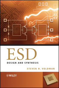
Electrostatic discharge (ESD) continues to impact semiconductor components and systems as technologies scale from micro- to nano-electronics.
This book studies electrical overstress, ESD, and latchup from a whole-chip ESD design synthesis approach. It provides a clear insight into the integration of ESD protection networks from a generalist perspective, followed by examples in specific technologies, circuits, and chips. Uniquely both the semiconductor chip integration issues and floorplanning of ESD networks are covered from a ‘top-down' design approach.
Look inside for extensive coverage on:
- integration of cores, power bussing, and signal pins in DRAM, SRAM, CMOS image processing chips, microprocessors, analog products, RF components and how the integration influences ESD design and integration
- architecturing of mixed voltage, mixed signal, to RF design for ESD analysis
- floorplanning for peripheral and core I/O designs, and the implications on ESD and latchup
- guard ring integration for both a ‘bottom-up' and ‘top-down' methodology addressing I/O guard rings, ESD guard rings, I/O to I/O, and I/O to core
- classification of ESD power clamps and ESD signal pin circuitry, and how to make the correct choice for a given semiconductor chip
- examples of ESD design for the state-of-the-art technologies discussed, including CMOS, BiCMOS, silicon on insulator (SOI), bipolar technology, high voltage CMOS (HVCMOS), RF CMOS, and smart power
- practical methods for the understanding of ESD circuit power distribution, ground rule development, internal bus distribution, current path analysis, quality metrics
ESD: Design and Synthesis is a continuation of the author's series of books on ESD protection. It is an essential reference for: ESD, circuit, and semiconductor engineers; design synthesis team leaders; layout design, characterisation, floorplanning, test and reliability engineers; technicians; and groundrule and test site developers in the manufacturing and design of semiconductor chips.
It is also useful for graduate and undergraduate students in electrical engineering, semiconductor sciences, and manufacturing sciences, and on courses involving the design of ESD devices, chips and systems. This book offers a useful insight into the issues that confront modern technology as we enter the nano-electronic era.
Sie lesen das E-Book in den Legimi-Apps auf:
Seitenzahl: 405
Veröffentlichungsjahr: 2011
Ähnliche
Contents
Cover
ESD Series By Steven H. Voldman
Title Page
Copyright
Dedication
About the Author
Preface
Acknowledgments
Chapter 1: ESD Design Synthesis
1.1 ESD Design Synthesis and Architecture Flow
1.2 ESD Design – The Signal Path and the Alternate Current Path
1.3 ESD Electrical Circuit and Schematic Architecture Concepts
1.4 Mapping Semiconductor Chips and ESD Designs
1.5 ESD Chip Architecture, and ESD Test Standards
1.6 ESD Testing
1.7 ESD Chip Architecture and ESD Alternative Current Paths
1.8 ESD Networks, Sequencing, and Chip Architecture
1.9 ESD Design Synthesis – Latchup-Free ESD Networks
1.10 ESD Design Concepts – Buffering – Inter-Device
1.11 ESD Design Concepts – Ballasting – Inter-Device
1.12 ESD Design Concepts – Ballasting – Intra-Device
1.13 ESD Design Concepts – Distributed Load Techniques
1.14 ESD Design Concepts – Dummy Circuits
1.15 ESD Design Concepts – Power Supply De-Coupling
1.16 ESD Design Concepts – Feedback Loop De-Coupling
1.17 ESD Layout and Floorplan-Related Concepts
1.18 ESD Design Concepts – Analog Circuit Techniques
1.19 ESD Design Concepts – Wire Bonds
1.20 Design Rules
1.21 Summary and Closing Comments
References
Chapter 2: ESD Architecture and Floorplanning
2.1 ESD Design Floorplan
2.2 Peripheral I/O Design
2.3 Lumped ESD Power Clamp in Peripheral I/O Design Architecture
2.4 Lumped ESD Power Clamp in Peripheral I/O Design Architecture – Master/Slave ESD Power Clamp System
2.5 Array I/O
2.6 ESD Architecture – Dummy Bus Architectures
2.7 Native Voltage Power Supply Architecture
2.8 Mixed-Voltage Architecture
2.9 Mixed-Signal Architecture
2.10 Mixed-System Architecture – Digital and Analog CMOS
2.11 Mixed-Signal Architecture – Digital, Analog, and RF Architecture
2.12 Summary and Closing Comments
References
Chapter 3: ESD Power Grid Design
3.1 ESD Power Grid
3.2 Semiconductor Chip Impedance
3.3 Interconnect Failure and Dynamic on-Resistance
3.4 Interconnect Wire and Via Guidelines
3.5 ESD Power Grid Resistance
3.6 Power Grid Layout Design
3.7 ESD Specification Power Grid Considerations
3.8 Power Grid Design Synthesis – ESD Design Rule Checking Methods
3.9 Summary and Closing Comments
References
Chapter 4: ESD Power Clamps
4.1 ESD Power Clamps
4.2 Design Synthesis of ESD Power Clamps
4.3 Design Synthesis of ESD Power Clamp – The ESD Power Clamp Shunting Element
4.4 ESD Power Clamp Issues
4.5 ESD Power Clamp Design
4.6 ESD Power Clamp Design Synthesis – Bipolar ESD Power Clamps
4.7 Master/Slave ESD Power Clamp Systems
4.8 Summary and Closing Comments
References
Chapter 5: ESD Signal Pin Networks Design and Synthesis
5.1 ESD Signal Pin Structures
5.2 ESD Input Structures – ESD and Bond Pads Layout
5.3 ESD Design Synthesis and Layout of MOSFETs
5.4 ESD Design Synthesis and Layout of Diodes
5.5 ESD Design Synthesis of SCRs
5.6 ESD Design Synthesis and Layout of Resistors
5.7 ESD Design Synthesis of Inductors
5.8 Summary and Closing Comments
References
Chapter 6: Guard Ring Design and Synthesis
6.1 Guard Ring Design and Integration
6.2 Guard Ring Characterization
6.3 Semiconductor Chip Guard Ring Seal
6.4 I/O to Core Guard Rings
6.5 I/O to I/O Guard Rings
6.6 Within I/O Guard Rings
6.7 ESD Signal Pin Guard Rings
6.8 Library Element Guard Rings
6.9 Mixed-Signal Guard Rings – Digital to Analog
6.10 Mixed-Voltage Guard Rings – High Voltage to Low Voltage
6.11 Passive and Active Guard Rings
6.12 Trench Guard Rings
6.13 TSV Guard Rings
6.14 Guard Ring DRC
6.15 Guard Rings and Computer Aided Design Methods
6.16 Summary and Closing Comments
References
Chapter 7: ESD Full-Chip Design Integration and Architecture
7.1 Design Synthesis and Integration
7.2 Digital Design
7.3 Custom Design vs. Standard Cell Design
7.4 Memory ESD Design
7.5 Microprocessor ESD Design
7.6 Application-Specific Integrated Circuits
7.7 CMOS Image Processing Chip Design
7.8 Mixed-Signal Architecture
7.9 Summary and Closing Comments
References
Index
ESD Series By Steven H. Voldman
ESD: Design and Synthesis
ISBN: 9780470685716
March 2011
ESD: Failure Mechanisms and Models
ISBN: 9780470511374
July 2009
Latchup
ISBN: 9780470016428
December 2007
ESD: RF Technology and Circuits
ISBN: 9780470847558
September 2006
ESD: Circuits and Devices
ISBN: 9780470847541
November 2005
ESD: Physics and Devices
ISBN: 9780470847534
September 2004
Upcoming titles:
ESD Basics: From Semiconductor Manufacturing to Use
ESD: Test and Characterization
This edition first published 2011
© 2011 John Wiley & Sons, Ltd
Registered office
John Wiley & Sons Ltd, The Atrium, Southern Gate, Chichester, West Sussex, PO19 8SQ, United Kingdom
For details of our global editorial offices, for customer services and for information about how to apply for permission to reuse the copyright material in this book please see our website at www.wiley.com.
The right of the author to be identified as the author of this work has been asserted in accordance with the Copyright, Designs and Patents Act 1988.
All rights reserved. No part of this publication may be reproduced, stored in a retrieval system, or transmitted, in any form or by any means, electronic, mechanical, photocopying, recording or otherwise, except as permitted by the UK Copyright, Designs and Patents Act 1988, without the prior permission of the publisher.
Wiley also publishes its books in a variety of electronic formats. Some content that appears in print may not be available in electronic books.
Designations used by companies to distinguish their products are often claimed as trademarks. All brand names and product names used in this book are trade names, service marks, trademarks or registered trademarks of their respective owners. The publisher is not associated with any product or vendor mentioned in this book. This publication is designed to provide accurate and authoritative information in regard to the subject matter covered. It is sold on the understanding that the publisher is not engaged in rendering professional services. If professional advice or other expert assistance is required, the services of a competent professional should be sought.
Library of Congress Cataloging-in-Publication Data
Voldman, Steven H.
ESD : Design and Synthesis / Steven H. Voldman.
p. cm.
Includes bibliographical references and index.
ISBN 978-0-470-68571-6 (hardback)
1. Semiconductors–Protection. 2. Integrated circuits–Protection. 3. Electrostatics. 4. Analog electronic systems–Design and construction. I. Title.
TK7871.85.V6525 2011
621.3815'2–dc22
2010048032
A catalogue record for this book is available from the British Library.
Print ISBN: 9780470685716
E-PDF ISBN: 9781119991144
O-book ISBN: 9781119991137
E-Pub ISBN: 9781119992653
To My Daughter
Rachel Pesha Voldman
About the Author
Dr Steven H. Voldman is the first IEEE Fellow in the field of electrostatic discharge (ESD) for “Contributions in ESD Protection in CMOS, Silicon On Insulator and Silicon Germanium Technology.” He received his B.S. in Engineering Science from the University of Buffalo (1979); a first M.S. EE (1981) from Massachusetts Institute of Technology (MIT); a second EE Degree (Engineer Degree) from MIT; an M.S. Engineering Physics (1986) and a Ph.D. in electrical engineering (EE) (1991) from the University of Vermont under IBM's Resident Study Fellow program.
He was a member of the IBM development team for 25 years, working on semiconductor device physics, device design, and reliability (e.g., soft error rate (SER), hot electrons, leakage mechanisms, latchup, and ESD). Steve Voldman has been involved in latchup technology development for 27 years. He worked on both technology and with-product development in bipolar SRAM, CMOS DRAM, CMOS logic, silicon on insulator (SOI), BiCMOS, silicon germanium (SiGe), RF CMOS, RF SOI, smart power, and image processing technologies. In 2008 he was a member of the Qimonda DRAM development team, working on 70, 58, and 48 nm CMOS technology. In 2008 he initiated a limited liability corporation (LLC), and worked at headquarters in Hsinchu, Taiwan for Taiwan Semiconductor Manufacturing Corportion (TSMC) as part of the 45 nm ESD and latchup development team. He is presently a Senior Principal Engineer working for the Intersil Corporation on ESD and latchup development.
Dr Voldman was Chairman of the SEMATECH ESD Working Group from 1995 to 2000. In his SEMATECH Working Group, attention focused on ESD technology benchmarking, the first transmission line pulse (TLP) standard development team, strategic planning, and JEDEC–ESD Association standards harmonization of the human body model (HBM) Standard. From 2000 to 2010, as Chairman of the ESD Association Work Group on TLP and very-fast TLP (VF-TLP), his team was responsible for initiating the first standard practice and standards for TLP and VF-TLP. Steve Voldman has been a member of the ESD Association Board of Directors and Education Committee. He initiated the “ESD on Campus” program, which was established to bring ESD lectures and interaction to university faculty and students internationally; the ESD on Campus program has reached over 32 universities in the United States, Singapore, Taiwan, Malaysia, the Philippines, Thailand, India, and China.
Dr Voldman teaches short courses and tutorials on ESD, latchup, and invention in the United States, China, Singapore, Malaysia, and Israel. He is a recipient of over 210 issued US patents, in the area of ESD and CMOS latchup. He has served as an expert witness in patent litigation cases associated with ESD and latchup.
Dr Voldman has also written articles for Scientific American and is an author of the first book series on ESD and latchup: ESD: Physics and Devices, ESD: Circuits and Devices, ESD:RF Technology and Circuits, a fourth text, Latchup, and a fifth text, ESD: Failure Mechanisms and Models. He is also a contributor to the book Silicon Germanium: Technology, Modeling and Design. There are international Chinese editions of the book ESD: Circuits and Devices and the text ESD: RF Technology and Circuits. He is also a chapter contributor to the text Nanoelectronics: Nanowires, Molecular Electronics, and Nano-devices.
Preface
The text ESD: Design and Synthesis is targeted at the semiconductor chip “architect”, team lead floorplan engineer, circuit designer, design layout support, ESD engineer, and computer aided design (CAD) integration team. In this text, a balance is established between design synthesis, design integration, layout engineering, and design checking and verification.
The first goal of the text ESD: Design and Synthesis is to teach the “art” of ESD chip design for a semiconductor chip.
The second goal is to demonstrate a step-by-step process to provide ESD protection to a semiconductor chip. The flow of the text addresses floorplanning, architecture, power rails, ESD networks for power rails, ESD signal pin solutions, guard rings, and examples of implementations. This flow is significantly different from the approach taken in most texts, but is the actual flow of how a design team proceeds through the ESD implementation.
The third goal is to expose the reader to the growing number of architectures and concepts being discussed today. Examples of DRAM, SRAM, image processing chips, microprocessors, mixed-voltage to mixed-signal applications, and floorplans will be shown.
The fourth goal is to address topics that are not discussed in other ESD textbooks. These topics include power bus architecture, guard rings, and floorplanning. For many ESD engineers and circuit designers, this is common knowledge; for others, it is not. A significant part of the ESD design and synthesis is spent on placement, floorplans, and integration.
This text, ESD: Design and Synthesis, contains the following:
Chapter 1 introduces the reader to an overview of the language and fundamentals associated with ESD design. In this chapter, ESD concepts are introduced from layout, circuits, to design rule checking. A “sampler” of concepts is laid out to the reader, to begin viewing the ESD design synthesis from a broader perspective. ESD design synthesis extends from the smallest contact, to full-chip integration. With this awareness, it is possible to realize the extent of the ESD design discipline in semiconductor design.For the next chapters, the text is structured as primarily a “top-down” ESD approach. This starts with floorplanning, bus architecture, ESD power clamps, ESD input circuits, and guard rings. The text will close with more examples of floorplanning and design integration. Most previous ESD texts focus on a “bottom-up” approach to ESD design integration; in “real-life” semiconductor integration, it typically starts from the “top down”.
Chapter 2 discusses chip architectures. In this chapter, the discussion focuses on ESD architecture and floorplan concepts. The chapter focuses on “peripheral I/O” and “array I/O” architectures, and how they influence the placement of the various elements for the whole-chip design integration. The chapter addresses native-voltage, mixed-voltage, and mixed-signal chip integration.Chapter 3 focuses on power grid design. In this chapter, the discussion continues to address issues associated with full-chip ESD design synthesis. The chapter focuses on the interconnects, power grid layout, and design itself. It addresses interconnect robustness, interconnect failure, and key metrics in the whole-chip ESD design synthesis. The chapter addresses the issue of integration with the ESD power clamps. This naturally flows into the next chapter.Chapter 4 addresses ESD power clamps on power domains and power pads. In this chapter, ESD power clamp circuits are discussed. ESD power clamp classification, key parameters, issues, and specific designs are discussed. How the ESD power clamps are integrated with the semiconductor chip will become more apparent.Chapter 5 focuses on ESD signal pad networks. In this chapter, ESD signal pin device layout and integration with bond pads are discussed. ESD signal pin classification, key parameters, issues, and specific designs are covered. The chapter focuses on ESD integration with the bond pad, from structures next to pads, adjacent to bond pad, partially-under, and under bond pads. All types of arrangements and orientation tradeoffs will be discussed. The chapter focuses on device layout and integration.Chapter 6 focuses on guard rings and guard ring integration. In this chapter, a “top-down” design synthesis approach for guard rings is shown for a semiconductor chip, starting with the seal ring, to domains, standard cell-to-standard cell, within-standard cell, and down to the individual devices. A “bottom-up” approach starts with the individual devices and works its way up to the full-chip implementation. Special structures and cases are shown as examples of how to further isolate both domains and devices. A small taste is given to show what is possible with the guard ring design synthesis and integration with both devices to full-chip implementations.Chapter 7 provides examples of different chip floorplans and architectures. In this chapter, the focus is on examples of design synthesis in full-chip implementations. Examples of DRAM, SRAM, microprocessors, mixed-voltage, mixed-signal, and RF applications will be shown. As part of the ESD design synthesis, the layout is key to a successful design implementation for both ESD and CMOS latchup. These examples will provide some understanding of the challenges in the ESD full-chip integration issues. By combining the knowledge of Chapters 1 through 6 with this chapter, the whole-chip design strategy should be better understood for any semiconductor chip architecture perspective.This text is part of an ESD book series on electrostatic discharge protection. To establish a strong knowledge of ESD protection, it is advisable to read the other texts on ESD and latchup as well. For this text, ESD: Design and Synthesis, hopefully we have covered the trends and directions of ESD design synthesis.
Enjoy the text, and enjoy the subject of ESD design synthesis.
Baruch HaShem (B”H) Dr Steven H. Voldman IEEE Fellow
Acknowledgments
In the area of ESD and latchup design, I would like to acknowledge the years of support from the SEMATECH, the ESD Association, the IEEE, and the JEDEC organizations. I would like to thank the IBM Corporation, Qimonda, Taiwan Semiconductor Manufacturing Corporation (TSMC), and the Intersil Corporation. This text comes from 30 years of working with bipolar memory, DRAM memory, SRAM, NVRAMs, microprocessors, ASICs, mixed-voltage, mixed-signal, RF, and power applications. I was fortunate to work in a wide number of technology teams, and with a wide breadth of customers. I was very fortunate to work in bipolar memory, CMOS DRAM, CMOS logic, ASICs, silicon on insulator (SOI), and silicon germanium (SiGe) from 1 μm to 45 nm technologies. I was very fortunate to be a member of talented technology and design teams that were innovative, intelligent, and inventive. This provided the opportunity to explore experimental concepts, and try new ideas in ESD design in applications and products.
I would like to thank the institutions that allowed me to teach and lecture at conferences, symposiums, industry, and universities; this gave me the motivation to develop the texts. I would like to thank faculty at the following universities: MIT, Stanford University, University of Central Florida (UCF), University Illinois Urbana-Champaign (UIUC), University of California Riverside (UCR), University of Buffalo, National Chiao Tung University (NCTU), Tsin Hua University, National Technical University of Science and Technology (NTUST), National University of Singapore (NUS), Nanyang Technical University (NTU), Beijing University, Fudan University, Shanghai Jiao Tung University, Zheijang University, Universiti Sains Malaysia, Chulalongkorn University, Mahanakorn University, Kasetsart University, Thammasat University, and Mapua Institute of Technology.
I would like to thank – for the years of support and the opportunity to provide lectures, invited talks, and tutorials – the Electrical Overstress/Electrostatic Discharge (EOS/ESD) Symposium, the International Reliability Physics Symposium (IRPS), the Taiwan Electrostatic Discharge Conference (T-ESDC), the International Electron Device Meeting (IEDM), the International Conference on Solid-State and Integrated Circuit Technology (ICSICT), and the International Physical and Failure Analysis (IPFA) in Singapore.
I would like to thank my many friends for 20 years in the ESD profession – Professor Ming Dou Ker, Professor J.J. Liou, Professor Albert Wang, Professor Elyse Rosenbaum, Timothy J. Maloney, Charvaka Duvvury, Eugene Worley, Robert Ashton, Yehuda Smooha, Vladislav Vashchenko, Ann Concannon, Albert Wallash, Vessilin Vassilev, Warren Anderson, Marie Denison, Alan Righter, Andrew Olney, Bruce Atwood, Jon Barth, Evan Grund, David Bennett, Tom Meuse, Michael Hopkins, Yoon Huh, Keichi Hasegawa, Nathan Peachey, Kathy Muhonen, Augusto Tazzoli, Gaudenzio Menneghesso, Marise BaFleur, Jeremy Smith, Nisha Ram, Swee K. Lau, Tom Diep, Lifang Lou, Stephen Beebe, Michael Chaine, Pee Ya Tan, Theo Smedes, Markus Mergens, Christian Russ, Harold Gossner, Wolfgang Stadler, Ming Hsiang Song, J.C. Tseng, J.H. Lee, Michael Wu, Erin Liao, Jim Vinson, Jean-Michel Tschann, David Swenson, Donn Bellmore, Ed Chase, Doug Smith, W. Greason, Stephen Halperin, Tom Albano, Ted Dangelmayer, Terry Welsher, John Kinnear, and Ron Gibson. I would also like to thank graduate students who are engaged in the study of ESD protection: Tze Wee Chen, Shu Qing Cao, Slavica Malobabic, David Ellis, Blerina Aliaj, and Lin Lin.
I would like to thank the ESD Association office for support in the area of publications, standards developments, and conference activities. I would also like to thank the publisher and staff of John Wiley and Sons, for including the text ESD: Design and Synthesis as part of the ESD book series.
To my children, Aaron Samuel Voldman and Rachel Pesha Voldman, good luck to both of you in the future.
To my wife, Annie Brown Voldman, thank you for the support of years of work.
And to my parents, Carl and Blossom Voldman.
Baruch HaShem (B”H)
Dr Steven H. Voldman IEEE Fellow
Chapter 1
ESD Design Synthesis
1.1 ESD Design Synthesis and Architecture Flow
In the ESD design synthesis process, there is a flow of steps and procedures to construct a semiconductor chip [1–13]. In many cases, the floorplanning process is a function of the type of semiconductor chip. The following design synthesis procedure is an example of an ESD design flow needed for semiconductor chip implementations:
I/O, Domains and Core Floorplan: Define floorplan of regions of cores, domains, and peripheral I/O circuitry.I/O Floorplan: Define area and placement for I/O circuitry.ESD Signal Pin Floorplan: Define ESD area and placement.ESD Power Clamp Network Floorplan: Define ESD power clamp area and placement for a given domain.ESD Domain-to-Domain Network Floorplan: Define ESD networks between the different chip domains area and placement for a given domain.ESD Signal Pin Network Definition: Define ESD network for the I/O circuitry.ESD Power Clamp Network Definition: Define ESD power clamp network within a power domain.Power Bus Definition and Placement: Define placement, bus width, and resistance requirements for the power bus.Ground Bus Definition and Placement: Define placement, bus width, and resistance requirements for the ground bus.I/O to ESD Guard Rings: Define guard rings between I/O and ESD networks.I/O Internal Guard Rings: Define guard rings within the I/O circuitry.I/O External Guard Rings: Define guard rings between I/O circuitry and adjacent external circuitry.1.1.1 Top-Down ESD Design
In the ESD design synthesis, the implementation can be thought of as a “top-down ESD design” process. Figure 1.1 is an example of a “top-down ESD design flow.” In the ESD design synthesis process, there is a flow of steps and procedures to construct a semiconductor chip. In my experience, in the planning stages of a semiconductor chip, the circuit team leader addresses the ESD design synthesis from a procedure as shown. With a “top-down ESD design synthesis” the integration, placement, sizing, and requirements are addressed. This process will be independent of whether the semiconductor chip is for digital logic [1–7, 11], analog design [14, 31–33], power electronics [26–30, 35–38], or radio frequency applications [8, 39–41].
Figure 1.1 Top-down ESD design flow
1.1.2 Bottom-Up ESD Design
In the ESD design synthesis, the implementation can also be addressed as a “bottom-up ESD design” process. Figure 1.2 is an example of a “bottom-up ESD design flow.” In a bottom-up ESD design synthesis process, the circuits are defined, and the corresponding ESD networks.
Figure 1.2 Bottom-up ESD design flow
One of the difficulties of ESD and the latchup design synthesis process is that the ESD design synthesis requires some “top-down” procedures, some “bottom-up” thinking, and integration. This will become more apparent throughout this text.
1.1.3 Top-Down ESD Design – Memory Semiconductor Chips
In the ESD design synthesis of a memory chip, the thought process is a “top-down ESD design” process, with the floorplanning driven by the array region. These designs are “array-dominated” designs, with the focus on the array [7]. The I/O region is limited in physical area, and the architecture is driven by the number of output pins, how to integrate it with the packaging, and how to support the I/O and ESD in the least amount of space. Figure 1.3 is an example of a “top-down ESD design flow” for a memory chip.
Figure 1.3 Top-down ESD design flow – memory
1.1.4 Top-Down ESD Design – ASIC Design System
In the ESD design synthesis of an applications-specific IC (ASIC) architecture, the procedure for the ESD design integration is significantly different. In the ASIC environment, the chip size, the number of I/O, and its ESD integration is dependent on the chip size. In this “top-down” methodology, the number of I/O, supported bus locations, placement of the I/O cells, integration of the ESD elements, and power are all synthesized in a different flow. Figure 1.4 is an example of a “top-down ESD design flow” for an ASIC methodology.
Figure 1.4 Top-down ESD design flow – ASICs
1.2 ESD Design – The Signal Path and the Alternate Current Path
In semiconductor chip design, the role of a semiconductor chip is to receive a signal, process the signal, and transmit the signal.
In ESD design synthesis, the role of the ESD network solution is to establish an alternate current path to avoid damage along the signal path that impacts its function or operation characteristics [7, 11]. As a result, simplistically, the ESD network must transmit the ESD current out of the sensitive signal path to an alternative path or current loop. This is achieved by diverting the ESD current to the power grid, or the ground plane. The fundamental requirements along the alternative current path are as follows:
An alternative current path must exist between any signal pin and any grounded reference (e.g., signal pin, power pin, ground pin).An ESD element must divert the ESD current to the power plane or ground plane.An ESD element must be able to transmit the ESD current to the power rail or ground rail without damage (to some specification level).The power rail and ground rail must be able to source the ESD current without damage (to some specification level).The alternative current path must achieve the ESD current discharge to the grounded reference to some specification level prior to damage along the signal path.To achieve this objective, there are some conditions on the alternative current path:
ESD networks are required to address both positive and negative polarity events.The ESD network must have low turn-on voltage and low resistance prior to destruction of the circuitry along the signal path.The power grid and the ground rail resistance must be sufficiently low to avoid IR voltage drops.Bi-directional electrical connectivity must exist, providing an alternative current path between all independent rails through ESD networks, or other means (e.g., circuitry, inductors, bond wires, packaging, etc.).Figure 1.5 shows an example of a semiconductor high-level schematic of the chip architecture. The figure highlights the signal path and the alternative ESD current path created by the ESD networks.
Figure 1.5 The signal path and alternative ESD current path
1.3 ESD Electrical Circuit and Schematic Architecture Concepts
In this section, discussion of ESD from a chip architecture, and the electrical schematic viewpoint will be shown. What are the ideal characteristics that we are looking for from an ESD network? What are the ideal characteristics from a frequency domain perspective? How is the chip architecture related to the testing procedure and the events that occur in a real chip?
1.3.1 The Ideal ESD Network and the Current–Voltage DC Design Window
The DC I–V characteristics may determine the “on” and “off” characteristics of the ESD network during functional operation, and its ESD effectiveness as an ESD network to protect other circuitry. An ideal ESD network has the following characteristics [7, 11]:
The ESD device, circuit, or network is “off” during the DC functional regime between signal levels between the most negative power supply voltage and the most positive power supply (associated with the signal pin).The ESD network has an “infinite resistance” when in the “off” state, which can be expressed asThe ESD network is “on” during voltage excursions that undershoot below the most negative power supply, or voltage excursions that overshoot the most positive power supply (during ESD testing).
The ESD network has a “zero resistance” whenThe ESD network operation extends beyond the “electrical safe-operation area” (electrical SOA) in DC voltage level or DC current level [26–30].
The ESD network operation does not extend beyond a “thermal safe-operation area” (thermal SOA) in DC voltage level or DC current level [26–30].The ESD network operation does not reach the current-to-failure, voltage-to-failure, or power-to-failure prior to the ESD specification level objective [15–30].ESD networks can consist of I–V characteristics of the following form:
Step function I–V characteristics.S-type I–V characteristics.N-type I–V characteristics.Step function I–V characteristics have a single “off” state as the structure is biased. At some voltage value, the device is “on.” For example, a diode element has a step function I–V characteristic and is suitable for ESD protection. In the case of a diode element, the ideality is a function of the on-resistance of the diode element.
1.3.2 The ESD Design Window
In the defining of an ESD network, there is a desired range of operation. The “ESD design window” is the region of desired operation on a current–voltage (I–V) plot (Figure 1.6). On the I–V plot, there is a region defined for functional operation of the semiconductor chip. The application voltage is designated as from a voltage of V = 0 to V = VDD. On the x-axis, there is an absolute maximum voltage (also known as ABS MAX). On the y-axis, there is an operational current and an absolute current magnitude which the application must remain below without damage. The operational current–voltage range forms a rectangular region on the I–V plot. The ESD network must operate between the VDD power supply and the absolute maximum voltage. On the current axis, the ESD network must discharge as high as possible to avoid the failure of the semiconductor component. The ESD current discharge should achieve the ESD specification levels. Hence, there is a region in which the ESD network is to operate without interfering with functional operation, but must discharge enough current prior to destruction of the semiconductor chip. In addition, the current magnitude must exceed the latchup current criteria for voltages lower than the power supply voltage.
Figure 1.6 ESD design window and SOA
Figure 1.7 shows an example of a diode in the ESD design window. Because of the non-ideality of the diode element, there is a region where the DC voltage of the semiconductor devices in the technology are exceeded.
Figure 1.7 ESD design window for an ESD device (e.g., diode I–V characteristic)
S-type characteristics are semiconductor devices or circuits that have two current states for a given voltage state. For example, an n-channel MOSFET or silicon-controlled rectifier (e.g., pnpn device) has an S-type I–V characteristic. Figure 1.8 shows an example of an n-channel MOSFET in a MOSFET drain-to-source configuration in an ESD design window. To utilize the MOSFET as an ESD network, the MOSFET snapback must occur within the current–voltage window of the technology limits of its safe operation area (SOA) of the other structures in the technology.
Figure 1.8 ESD design window for an S-type I–V characteristic ESD device
Figure 1.9 shows the ESD design window as a function of the technology generation. As observed, as the power supply voltage is reduced, the ESD design window decreases for successive technology generations.
Figure 1.9 ESD design window as a function of technology generation
1.3.3 The Ideal ESD Networks in the Frequency Domain Design Window
From an RF ESD design perspective, the characteristics of an RF ESD design are focused on its RF characteristics at the RF application frequency [8]. Figure 1.10 shows an example of ESD phenomenon frequencies, and RF application frequencies. RF applications are now faster than ESD phenomena for applications that exceed 5 GHz. This opens opportunities for unique RF ESD design implementations [8].
Figure 1.10 RF application frequency and ESD pulse event frequency
From an RF perspective, the ideal RF ESD network has the following features [8]:
An ideal RF ESD network would have zero impedance during an ESD pulse.An ideal RF ESD network has infinite impedance during RF functional applications.An ideal RF ESD network during RF functional operation would not be a function of the current or voltage conditions.An ideal RF ESD network during RF functional operation is not temperature dependent.Hence, from the frequency design window for RF ESD design, it is desirable to have an RF ESD network with zero impedance at low frequencies (e.g., HBM, MM, and CDM phenomenon regime below 5 GHz), and high impedance in the application frequency (e.g., RF application frequency regime).
Figure 1.11 shows the RF ESD frequency design window, and an ideal impedance characteristic imposed on the window. In a frequency regime below the CDM phenomenon, the ideal ESD impedance would be high during DC functional response, with zero impedance during an ESD event. At high frequencies, in the range of the RF application frequency, the impedance would have a high value (Figure 1.12).
Figure 1.11 RF ESD frequency domain design window and the RF ESD device impedance
Figure 1.12 Design methodology vs. application frequency
1.4 Mapping Semiconductor Chips and ESD Designs
In semiconductor chip design, products are mapped from technology-to-technology for improved productivity. Designs are mapped from one foundry to another, and from technology generation to technology generation. Designs undergo re-mapping from bipolar to CMOS [6–8, 39–41], and CMOS to SOI processes [6–8, 11, 41–44]. Additionally, there are both generational changes as well as productivity “shrinks.” In this process the ESD design synthesis is influenced.
1.4.1 Mapping Across Semiconductor Fabricators
In semiconductor development, it is not uncommon to implement the same semiconductor chip design in multiple semiconductor fabrication facilities in today's business environments. Mapping of a semiconductor chip can occur in the following manner:
Multiple semiconductor fabricators using the same technology.Multiple semiconductor fabricators using different technologies.In the case of a utilization of multiple semiconductor fabricators, two different manufacturing lines can satisfy the same electrical specifications but in fact have unique features that influence the ESD semiconductor design. Semiconductor variations that influence ESD results can be as follows:
Incoming wafer specifications for doping concentration.Incoming wafer specifications for epitaxy thickness.Photolithography tool bias conditions.Etch bias conditions.In many manufacturing processes, the specifications contain only a lower-bound condition for some values. In other cases, although there is a range for a specification, there is variation within the specification window that can influence ESD results.
As an example, incoming wafers may be supplied from different vendors to different manufacturing facilities. Although the wafer specification is equivalent, the wafers may be “centered” differently within the specification window. In a p-/p++ substrate wafer, the epitaxial thickness may vary within the specification, as well as the measurement technique to control epitaxial thickness. In one case, a CMOS semiconductor chip was mapped into three different facilities on a p-/p++ wafer in a single-well semiconductor process. The ESD protection solution was a silicon controlled rectifier (SCR), whose triggering means the n-well-to-substrate breakdown. In the three different facilities, the breakdown voltages were different, leading to a different triggering voltage for the same semiconductor design. As a result, only one facility achieved the HBM ESD objective, whereas the other facilities did not.
To guarantee ESD equivalent results from fabricator-to-fabricator for a given technology, all electrical parameters that influence the ESD networks should be verified, and controlled to equivalent parameters. Secondly, ESD testing should be performed to determine the ESD pin distribution of the semiconductor product; this can be achieved by testing all signal and power pins to failure.
In the case of mapping across semiconductor fabricators of different semiconductor processes, the ESD robustness of all processes is not equivalent. Semiconductor process differences can influence the ESD circuits, and the functional circuits. All process variables can influence the ESD protection levels; which process features influence the product ESD robustness is dependent on the ESD circuit type used, and worst case ESD failure mechanism. To guarantee ESD equivalent results from fabricator-to-fabricator for a different technology, all electrical parameters that influence the ESD networks should be verified. Transmission line pulse (TLP) and human body model (HBM) measurements of the semiconductor device library and the ESD circuit library may be used to verify equivalency. Secondly, ESD testing should be performed to determine the ESD pin distribution of the semiconductor product; this can be achieved by testing all signal and power pins to failure.
Given that the semiconductor fabricators provide a set of ESD benchmark structures to quantify the semiconductor technology, and ESD TLP measurements, design adjustments can be made to the ESD circuit design and functional circuitry to compensate for differences between the semiconductor fabricators.
1.4.2 ESD Design Mapping Across Technology Generations
In semiconductor development, semiconductor chip designs are mapped from one technology generation to another for performance improvements, chip size reduction, and cost.
In the ESD design synthesis of mapping across technology generations, the semiconductor design can undergo different design and architectural conditions. In the re-mapping from one technology generation to another technology generation, the type of mapping can influence the ESD design. Two mapping processes are as follows:
Lower power supply voltage for both peripheral I/O and core circuitry.Maintain the power supply voltage on the peripheral I/O, but reduced core circuitry supply voltage.In the first case, the reduction of the power supply voltage for the entire semiconductor chip can lead to both circuit topology and technology differences that influence the ESD results. With the lowering of the power supply voltage, given that the first generation contained elements in series, these can be reduced with the re-mapping process. With a reduction of the series elements in the ESD networks, ESD improvement can be obtained.
With the technology scaling, the physical dimensions of the devices are reduced. Dimensional scaling of the technology can influence the ESD results as follows:
Lower dielectric breakdown voltage.Lower MOSFET and bipolar snapback voltage.Different current-to-failure.Different power-to-failure.Different voltage-to-failure.With the technology scaling, the changes in the ESD robustness can be lower or higher, depending on the decisions of the doping concentration and film thickness. In the case where the ESD robustness is reduced, design modifications can be made to improve the product ESD results. The design modification can be the physical size of the ESD networks, innovation, or novelty.
In the second case, the product must maintain the same external or application voltages in the scaled technology. To obtain the density advantage of the scaled technology, the semiconductor chip design synthesis may take various directions:
Single power supply supporting both mixed voltage interface circuitry.Single power supply, and regulated voltage for core circuitry.Multiple power supply pins.In the case of many product applications, the peripheral circuitry is required to receive or transmit signals to semiconductor chips different from the native voltage of semiconductor technology. The ESD architecture and design synthesis are highly influenced by these conditions in both digital, analog, and power designs.
1.4.3 Mapping from Bipolar Technology to CMOS Technology
In the mapping of a design from bipolar technology to CMOS technology, the ESD design must be adjusted since the bipolar transistors differ significantly from CMOS MOSFET transistors [6–8, 14]. Bipolar transistors operate as vertical bulk devices, whereas MOSFET transistors operate as lateral surface devices. As a result, bipolar transistors provide lower current densities, and are more suitable for power and ESD implementations. Bipolar transistors can also be utilized as forward biased elements, or reverse breakdown devices, providing flexibility in the different types of implementations.
In the bipolar implementations, bipolar transistors are utilized for ESD protection on the signal pins, and the power rails. Bipolar transistors are typically used in collector-to-emitter configuration. Bipolar transistors are also used in diode configuration (e.g., base-collector, or emitter-base). In the mapping of a schematic design from bipolar technology to CMOS technology, bipolar diodes can be mapped directly as CMOS-based p–n diode elements formed out of diffusions and wells [8]. ESD inputs that are grounded base bipolar circuits (e.g., collector connected to input, and emitter connected to ground) can be mapped into grounded gate MOSFETs. ESD power clamps between power rails can be mapped from bipolar collector–emitter configured networks to grounded-gate triggered MOSFET power clamps or RC-triggered MOSFET power clamps.
One of the critical differences is that the size and layout of the implementations are significantly different between the bipolar elements and the CMOS elements (Figure 1.13). Since the bipolar transistors are bulk devices, and MOSFETs are surface devices, the perimeter and width of the MOSFET ESD devices are increased to achieve the same levels of ESD robustness.
Figure 1.13 Mapping of bipolar to CMOS technology
1.4.4 Mapping from Digital CMOS Technology to Mixed Signal Analog–Digital CMOS Technology
In the mapping of a semiconductor chip from a digital CMOS technology to a digital–analog technology, the ESD design synthesis, architecture, and physical elements may require adjustments [14]. With the introduction of an analog domain, modifications are needed in the architecture of the semiconductor chip. Digital and analog domains are required to be established, as well as ESD protection for each independent power domain. In addition, added ESD protection is needed for signal lines that cross both domains. Digital designs also typically have simple connections, whereas analog networks typically have a higher number of electrical connections to many different sub-functions.
Another key difference is that the floorplanning of the semiconductor chip into separated analog and digital domains influences the placement of the physical elements and the electrical connections. In addition, the analog design layout may consist of different analog design layout considerations of both active and passive elements; these practices will be discussed in later sections of the text.
1.4.5 Mapping from Bulk CMOS Technology to Silicon on Insulator (SOI)
For performance enhancements, CMOS designs can be mapped from bulk CMOS to silicon on insulator (SOI) technology [6, 7, 11, 43, 44]. In the mapping from a bulk CMOS technology to an SOI technology, modifications are required in both the functional circuitry and the ESD designs. Mapping of the ESD design will be dependent on the ESD device choice, the thickness of the silicon film, the isolation, the technology features, and technology type. Various forms of SOI technology exist:
Thin film partially depleted SOI (PD-SOI) MOSFET.Thick body partially depleted SOI (PD-SOI) MOSFET.Thin body fully depleted SOI (FD-SOI) MOSFET.SOI FinFET technology.Bipolar CMOS–DMOS SOI.In partially depleted SOI (PD-SOI) technology, the MOSFET junctions extend to the buried oxide (BOX) region [6, 7]. The silicon film on the BOX region is on the scale of the MOSFET junction depth. Isolation is formed, which extends from the device surface to the BOX film. The introduction of the BOX film, and integration with the isolation technology, leads to the elimination of all desired and undesired parasitic elements under the isolation structure. From an ESD perspective, all undesired parasitic elements are eliminated. For I/O and ESD elements, isolating guard rings are no longer required. External latchup and internal latchup is no longer an issue in thin body PD-SOI.
In the re-mapping process from CMOS to PD-SOI, the diode elements and SCRs can not conduct current vertically, or under the isolation region; this leads to modification of the ESD networks to allow a conduction path. Lateral elements will be required for ESD protection due to the elimination of any active device under the isolation structure. As a result, new ESD structures will be required.
For thick body PD-SOI, the buried oxide film extends under the well or buried layer depths and does not fully isolate the p-channel MOSFET and n-channel MOSFET devices. The isolation structure may extend to the buried oxide film, allowing separation of tubs and floating relative to the substrate wafer. As a result, in the re-mapping from CMOS to thick body SOI, ESD networks that utilize surface devices may not require design modification.
For bulk bipolar CMOS–DMOS (BCD) technology, the depth of the BOX region separates the devices from the substrate wafer, and provides isolation of the different device types. The devices that extend to the BOX region will be influenced in the mapping process. The BOX region will influence both the breakdown voltages and the current conduction. As a result, ESD networks will require modifications.
In the mapping from bulk CMOS to FinFET technology, the layout and design of all devices in the technology are modified [11]. ESD networks will also be required to be modified due to the means of current distribution in the FinFET structure (Figure 1.14).
Figure 1.14 Mapping of bulk CMOS to SOI technology
1.4.6 ESD Design – Mapping CMOS to RF CMOS Technology
Today, many designs are being defined from a CMOS base to an RF CMOS base technology [8, 11, 39–41]. CMOS-based designs are typically developed as a custom layout, including the ESD networks. In the CMOS ESD designs, the designs are not scalable elements and typically do not have scalable models.
Ironically, today many applications are using RF CMOS technology for the usage of the scalable models and AC models. In many application spaces, RF CMOS foundry technologies are being used for the higher-quality models. For analog design, small and large signal models are needed in the linear and the saturation region of the MOSFET devices, as well as in high-quality passive elements with good matching characteristics.
In the mapping of a digital or analog design into an RF CMOS technology, the ability to have better-quality AC models is available. For ESD design, it is also possible to have ESD designs with scalable elements. ESD designs can be constructed from parameterized cell elements. The primitive ESD design elements can be hierarchically defined, forming hierarchical parameterized cell ESD networks. Such elements can be constructed in a Cadence™ design environment [8]. By using an RF CMOS technology, the design synthesis environment allows for this ESD design strategy.
In the mapping of CMOS to RF CMOS, the circuit topology of the RF networks will introduce passive elements, such as capacitors and inductors [8]. Inductors and capacitors are used for DC isolation, input and output matching, filters, and matching. Inductors and capacitors are preferred resistor elements. As a result, in the re-mapping of circuits to RF CMOS, resistor elements are replaced by both capacitor and inductor elements. In ESD networks, typical CMOS ESD solutions (such as resistor ballasting and series resistor elements) are replaced with inductive and inductive–capacitive techniques.
In addition, in the ESD design synthesis, the RF circuits and ESD networks must be co-synthesized [8]. ESD-RF design co-synthesis is needed to achieve the RF performance objectives and matching characteristics.
1.5 ESD Chip Architecture, and ESD Test Standards
The ESD standards are written to test the ESD robustness between possible “events.” These events contain two features. The first feature is a given waveform. The second feature is the possible interactions that can occur within a semiconductor chip. The possible interaction is the case that a given pin receives an ESD event, and a second pin is the reference ground. The first feature tests the nature of the pulse, and the second feature is evaluating the current paths. In the ESD standards, different procedures exist in application of the ESD pulse to the pin or package, as well as the “pin combinations.”
1.5.1 ESD Chip Architecture and ESD Testing
The pin combinations are evaluating the ESD robustness of the possible paths, which in essence is testing the existence of a suitable ESD current path to discharge the ESD current. As a result, the chip architecture must be constructed to establish current paths, alternate current paths, and “elements” within the path that are suitable to discharge the ESD current. The elements in the path are the devices, circuits, and electrical interconnects within the path.
A key point is that for some of the ESD standards, the semiconductor chip architecture is structured to satisfy the ESD pin combinations of the ESD test standard.
1.6 ESD Testing
In this section, a brief discussion of ESD testing will be given, with relevance to ESD chip architecture. As stated in the last section, the architecture of the chip is structured to pass the ESD testing procedure. As a supplier, or customer, it is an expectation that a certain number of ESD test standards are performed, and achieve given objectives.
1.6.1 ESD Qualification Testing
Qualification testing to demonstrate ESD robustness is performed by the supplier, or customer. ESD testing is typically completed in the environment that it is shipped from the supplier to the customer. Figure 1.15 is an example of the ESD test flow. The ESD testing can be completed on wafer, bare die, or packaged components. The majority of the ESD testing standards are defined and structured to address the packaged component.
Figure 1.15 ESD test flow
1.6.2 ESD Test Models
ESD specifications contain different waveforms and pin combinations depending on the intent of the ESD event that the procedure is to simulate [47–82]. Component-level ESD test models include the following:
Human body model (HBM) [47–53].Machine model (MM) [54].Charged device model (CDM) [55].Socketed device model (SDM).Human metal model (HMM) [79–82].ESD system-level tests, presently being performed on chips, sub-systems, and systems, are as follows [56–64, 76–82]:
Charged board event (CBE).Cable discharge event (CDE) [56–64].IEC 61000-4-2 ESD pulse [76–79].Human metal model [79–82].Figure 1.16 is a chart demonstrating the evolution of testing in the semiconductor industry. The HBM test model was the first developed ESD specification for qualification of semiconductor devices. This was followed by the MM test specification, and CDM test specification. Today, there are additional test specifications at various phases of becoming ESD test standards.
Figure 1.16 ESD testing evolution
1.6.3 ESD Characterization Testing
ESD characterization tests that are being performed on wafers and on packages include the following [47–54, 65–75]:
Human body model (HBM) [47–53].Machine model (MM) [54].Transmission line pulse (TLP) [65–68].Very fast transmission line pulse (VF-TLP) [69–74].Ultra-fast transmission line pulse (UF-TLP) [75].Wafer-level HBM and MM testing can be performed as a two-pin test.
1.6.4 TLP Testing
ESD characterization tests that are being performed on wafers and on packages include the following [65–75]:
Transmission line pulse (TLP) [65–68].Very fast transmission line pulse (VF-TLP) [69–74].Ultra-fast transmission line pulse (UF-TLP) [75].In Figure 1.17, an example of a TLP system is shown. In a TLP system, a transmission line (TL) cable is charged by a high-voltage source. A switch is closed to apply the stress to the device-under-test (DUT). The TL pulse width is defined by the length of the cable in a given test system. The voltage and current are measured across the device under test as the pulse propagates through the device. There are various configurations of the TLP system. In some TLP systems, the configurations are such as to measure the reflected and transmitted signal through the device. A current and voltage value is determined in the device through averaging of the data in a “measurement window” within the pulse event.
Figure 1.17 TLP test system
A pulsed I–V characteristic can be constructed by increasing the voltage on the cable, and extracting the (I,V) data points in this successive step stress. Figure 1.18 shows an example of a TLP pulsed I–V characteristic. Each point represents a single pulse in the step stress, where the (I,V) point is an averaged measurement extracted from the measurement window.
Figure 1.18 TLP pulsed I–V characteristic
1.7 ESD Chip Architecture and ESD Alternative Current Paths
