179,99 €
Mehr erfahren.
- Herausgeber: John Wiley & Sons
- Kategorie: Wissenschaft und neue Technologien
- Sprache: Englisch
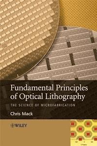
The fabrication of an integrated circuit requires a variety of physical and chemical processes to be performed on a semiconductor substrate. In general, these processes fall into three categories: film deposition, patterning, and semiconductor doping. Films of both conductors and insulators are used to connect and isolate transistors and their components. By creating structures of these various components millions of transistors can be built and wired together to form the complex circuitry of modern microelectronic devices. Fundamental to all of these processes is lithography, ie, the formation of three-dimensional relief images on the substrate for subsequent transfer of the pattern to the substrate. This book presents a complete theoretical and practical treatment of the topic of lithography for both students and researchers. It comprises ten detailed chapters plus three appendices with problems provided at the end of each chapter. Additional Information: Visiting href="http://www.lithoguru.com/textbook/index.html">http://www.lithoguru.com/textbook/index.html enhances the reader's understanding as the website supplies information on how you can download a free laboratory manual, Optical Lithography Modelling with MATLAB®, to accompany the textbook. You can also contact the author and find help for instructors.
Sie lesen das E-Book in den Legimi-Apps auf:
Seitenzahl: 916
Veröffentlichungsjahr: 2011
Ähnliche
CONTENTS
Preface
1 Introduction to Semiconductor Lithography
1.1 Basics of IC Fabrication
1.2 Moore’s Law and the Semiconductor Industry
1.3 Lithography Processing
Problems
References
2 Aerial Image Formation–The Basics
2.1 Mathematical Description of Light
2.2 Basic Imaging Theory
2.3 Partial Coherence
2.4 Some Imaging Examples Problems
Problems
References
3 Aerial Image Formation – The Details
3.1 Aberrations
3.2 Pupil Filters and Lens Apodization
3.3 Flare
3.4 Defocus
3.5 Imaging with Scanners Versus Steppers
3.6 Vector Nature of Light
3.7 Immersion Lithography
3.8 Image Quality
Problems
References
4 Imaging in Resist: Standing Waves and Swing Curves
4.1 Standing Waves
4.2 Swing Curves
4.3 Bottom Antireflection Coatings
4.4 Top Antireflection Coatings
4.5 Contrast Enhancement Layer
4.6 Impact of the Phase of the Substrate Reflectance
4.7 Imaging in Resist
4.8 Defining Intensity
Problems
References
5 Conventional Resists: Exposure and Bake Chemistry
5.1 Exposure
5.2 Post-Apply Bake
5.3 Post-exposure Bake Diffusion
5.4 Detailed Bake Temperature Behavior
5.5 Measuring the ABC Parameters Problems
Problems
References
6 Chemically Amplified Resists: Exposure and Bake Chemistry
6.1 Exposure Reaction
6.2 Chemical Amplification
6.3 Measuring Chemically Amplified Resist Parameters
6.4 Stochastic Modeling of Resist Chemistry
Problems
References
7 Photoresist Development
7.1 Kinetics of Development
7.2 The Development Contrast
7.3 The Development Path
7.4 Measuring Development Rates Problems
Problems
References
8 Lithographic Control in Semiconductor Manufacturing
8.1 Defining Lithographic Quality
8.2 Critical Dimension Control
8.3 How to Characterize Critical Dimension Variations
8.4 Overlay Control
8.5 The Process Window
8.6 H–V Bias
8.7 Mask Error Enhancement Factor (MEEF)
8.8 Line-End Shortening
8.9 Critical Shape and Edge Placement Errors
8.10 Pattern Collapse Problems
Problems
References
9 Gradient-Based Lithographic Optimization: Using the Normalized Image Log-Slope
9.1 Lithography as Information Transfer
9.2 Aerial Image
9.3 Image in Resist
9.4 Exposure
9.5 Post-exposure Bake
9.6 Develop
9.7 Resist Profile Formation
9.8 Line Edge Roughness
9.9 Summary Problems
Problems
References
10 Resolution Enhancement Technologies
10.1 Resolution
10.2 Optical Proximity Correction (OPC)
10.3 Off-Axis Illumination (OAI)
10.4 Phase-Shifting Masks (PSM)
10.5 Natural Resolutions
Problems
References
Appendix A Glossary of Microlithographic Terms
Appendix B Curl, Divergence, Gradient, Laplacian
B.1 Cross Product
B.2 Dot Product
B.3 Curl
B.4 Divergence
B.5 Gradient
B.6 Laplacian
B.7 Some Useful Identities
B.8 Spherical Coordinates
Appendix C The Dirac Delta Function
C.1 Definition
C.2 Properties and Theorems
Index
Copyright © 2007 John Wiley & Sons Ltd, The Atrium, Southern Gate, Chichester, West Sussex PO19 8SQ, England
Telephone (+44) 1243 779777
Email (for orders and customer service enquiries): [email protected] Visit our Home Page on www.wileyeurope.com or www.wiley.com
Reprint with corrections August 2008
All Rights Reserved. No part of this publication may be reproduced, stored in a retrieval system or transmitted in any form or by any means, electronic, mechanical, photocopying, recording, scanning or otherwise, except under the terms of the Copyright, Designs and Patents Act 1988 or under the terms of a licence issued by the Copyright Licensing Agency Ltd, 90 Tottenham Court Road, London W1T 4LP, UK, without the permission in writing of the Publisher. Requests to the Publisher should be addressed to the Permissions Department, John Wiley & Sons Ltd, The Atrium, Southern Gate, Chichester, West Sussex PO19 8SQ, England, or emailed to [email protected], or faxed to (+44) 1243 770620.
Designations used by companies to distinguish their products are often claimed as trademarks. All brand names and product names used in this book are trade names, service marks, trademarks or registered trademarks of their respective owners. The Publisher is not associated with any product or vendor mentioned in this book.
This publication is designed to provide accurate and authoritative information in regard to the subject matter covered. It is sold on the understanding that the Publisher is not engaged in rendering professional services. If professional advice or other expert assistance is required, the services of a competent professional should be sought.
The Publisher and the Author make no representations or warranties with respect to the accuracy or completeness of the contents of this work and specifically disclaim all warranties, including without limitation any implied warranties of fitness for a particular purpose. The advice and strategies contained herein may not be suitable for every situation. In view of ongoing research, equipment modifications, changes in governmental regulations, and the constant flow of information relating to the use of experimental reagents, equipment, and devices, the reader is urged to review and evaluate the information provided in the package insert or instructions for each chemical, piece of equipment, reagent, or device for, among other things, any changes in the instructions or indication of usage and for added warnings and precautions. The fact that an organization or Website is referred to in this work as a citation and/or a potential source of further information does not mean that the author or the publisher endorses the information the organization or Website may provide or recommendations it may make. Further, readers should be aware that Internet Websites listed in this work may have changed or disappeared between when this work was written and when it is read. No warranty may be created or extended by any promotional statements for this work. Neither the Publisher nor the Author shall be liable for any damages arising herefrom.
Other Wiley Editorial Offices
John Wiley & Sons Inc., 111 River Street, Hoboken, NJ 07030, USA
Jossey-Bass, 989 Market Street, San Francisco, CA 94103-1741, USA
Wiley-VCH Verlag GmbH, Boschstr. 12, D-69469 Weinheim, Germany
John Wiley & Sons Australia Ltd, 42 McDougall Street, Milton, Queensland 4064, Australia
John Wiley & Sons (Asia) Pte Ltd, 2 Clementi Loop #02-01, Jin Xing Distripark, Singapore 129809
John Wiley & Sons Ltd, 6045 Freemont Blvd, Mississauga, Ontario L5R 4J3, Canada
Wiley also publishes its books in a variety of electronic formats. Some content that appears in print may not be available in electronic books.
Anniversary Logo Design: Richard J. Pacifico
British Library Cataloguing in Publication Data
A catalogue record for this book is available from the British Library
ISBN 978-0-470-01893-4
To Susan, Sarah and Anna
Preface
There was a time when I was sure this book would never be finished. Believe it or not, I began working on it about 18 years ago, and for a long time it seemed that each year left me farther from completion (a consequence of working in a rapidly changing field). Several things conspired to finally make this book a reality. Ron Hershel, the closest person to a mentor I have known, gave me sage advice on writing a book: Dons’t try to write it all at once–instead, write and publish pieces of your book as journal articles over time, then collect them up when you have written enough. That advice has served me well, especially since I have been writing a quarterly column for Microlithography World since 1992. That approach helped me finish my first book, Inside PROLITH: A Comprehensive Guide to Optical Lithography Simulation, in 1997.
While I enjoyed finishing and publishing Inside PROLITH, my ambition was to write a more comprehensive university textbook on the topic of semiconductor lithography. I have been teaching a graduate level class on optical lithography at the University of Texas at Austin since 1991, using handouts in place of a real book. Each year I strove to add more material to make those notes more complete. But I ran into the same problem as before–new material in this quickly changing field was needed at a faster rate than I was writing.
I solved this problem in two ways. First, I began to focus solely on fundamental principles needed to understand the science of lithography. While lithography practice changes quickly, the fundamental principles underlying that practice do not. The result, though, is that this book has very little ‘practical’ advice, that is, descriptions of best practices in the industry. While such practical descriptions can be very useful, they also become dated very quickly. I hope that by focusing on fundamentals this book might be useful to the reader many years after it is purchased.
Secondly, I quit my job and worked on this book full-time (well, almost full time) for the final year before its completion. I hope that this admission doesn’t scare off the earnest would-be author, but the reality was, for me at least, that dedicated effort was required
to complete the project. Much of the material contained herein is, of course, a tutorial review of the published literature on lithography and related sciences. But a significant portion is new work, having never before been published. Thus, I hope that this book will contribute to the body of lithography literature mostly as a convenient repository of a useful portion of the collective knowledge in this field, but also as a repository for the information contained in various notebooks, files and scraps of paper scattered around my cluttered office.
While the length of the final book surprised even me, still, there are many fascinating and important topics in lithography that have been excluded for lack of space. In particular, rigorous treatment of electromagnetic scattering through the topography of a photomask is extremely important in lithography today, but goes without even a mention in the book. With respect to photoresist, etch resistance, spin coat rheology, adhesion, shelf life and quality control, resist formulations and defects all receive short shrift, and nothing is mentioned of top surface imaging or the various multilayer and nontraditional resist schemes. For those interested in imaging tools, the topics of geometrical optics, lens design, aberration measurement and tool component functions such as alignment, autofocus, stage motion, etc., are essentially ignored. The world of mask making is left to other books, as are the topics of chip design and design for manufacturability, despite their obvious impact on the field of lithography. Metrology, especially critical dimension metrology, is extremely important to lithography, since data from these measurements drive much of our knowledge of how lithography behaves. However, even though metrology deserves an entire chapter, I have left it out almost completely. Surprisingly to some, I have chosen not to cover an aspect of lithography very dear to me–lithography simulation. While the use of simulation is illustrated throughout the book, and of course a scientific description of lithography must necessarily serve as the foundation of a lithographic simulator, I have avoided the topic of the numerical solutions to the equations presented in the book as well as to the topics of model speed, accuracy and calibration. Finally, there is no effort to describe research into next generation lithography technologies, and no description of the many lithographic approaches that dons’t use projection optical imaging. Despite these glaring omissions, I still might be criticized for making the book too long, with too many topics, for use as a university text. I can only say that I have successfully covered most of the information contained in the book in a one semester course, with only the usual amount of grumbling from the affected students.
I am indebted to many, many people for their help with this book. In the 24 years that I have worked in the field of lithography I have been taught by many, many people. I couldns’t possible begin to count, let alone recount, the published works that have so greatly contributed to my understanding in this field. In fact, I will here issue a blanket apology to all those whose important works I have relied on but did not include in the references in the book. The lack of proper references is, I think, the biggest failure of this work, though I hope to be forgiven based on its format as a university textbook. I would also like to thank the students at the University of Texas at Austin and at Notre Dame whom I punished with early drafts of this book. Their feedback and experiences, good and bad, helped me to greatly improve the material and make it more suitable for the classroom.
There are many people who helped by reviewing chapters and providing feedback: Gary Bernstein, John Biafore, Robert Bunch, Jeff Byers, John Kulp and John Petersen
among others that I am sure I am forgetting. I would especially like to thank Warren Grobman who carefully read every chapter in the book and provided invaluable feedback, and Trey Graves who bravely defied Finmans’s Law of Mathematics and re-derived many of the equations in Chapters 2 and 3. I am indebted to Chris Sallee and KLA-Tencor for allowing me the use of the lithography simulator PROLITH, which I employed extensively in generating many of the figures found throughout the book.
As a final note, I encourage the interested reader to visit the web page for this book: www.lithoguru.com/textbook. There I will post errata and other information that might be useful to the reader, and information that might prove valuable to the professor interested in using this text as the basis for a university course.
Chris A. Mack
Austin, Texas
June, 2007
1
Introduction to Semiconductor Lithography
The fabrication of an integrated circuit (IC) involves a great variety of physical and chemical processes performed on a semiconductor (e.g. silicon) substrate. In general, the various processes used to make an IC fall into three categories: film deposition, patterning and semiconductor doping. Films of both conductors (such as polysilicon, aluminum, tungsten and copper) and insulators (various forms of silicon dioxide, silicon nitride and others) are used to connect and isolate transistors and their components. Selective doping of various regions of silicon allows the conductivity of the silicon to be changed with the application of voltage. By creating structures of these various components, millions (or even billions) of transistors can be built and wired together to form the complex circuitry of a modern microelectronic device. Fundamental to all of these processes is lithography, i.e. the formation of three-dimensional (3D) relief images on the substrate for subsequent transfer of the pattern into the substrate.
The word lithography comes from the Greek lithos, meaning stones, and graphia, meaning to write. It means quite literally writing on stones. In the case of semiconductor lithography, our stones are silicon wafers and our patterns are written with a lightsensitive polymer called a photoresist. To build the complex structures that make up a transistor and the many wires that connect the millions of transistors of a circuit, lithography and etch pattern transfer steps are repeated at least 10 times, but more typically 25 to 40 times to make one circuit. Each pattern being printed on the wafer is aligned to the previously formed patterns as slowly the conductors, insulators and selectively doped regions are built up to form the final device.
The importance of lithography can be appreciated in two ways. First, due to the large number of lithography steps needed in IC manufacturing, lithography typically accounts for about 30% of the cost of manufacturing a chip. As a result, IC fabrication factories (‘fabs’) are designed to keep lithography as the throughput bottleneck. Any drop in output of the lithography process is a drop in output for the entire factory. Second, lithography tends to be the technical limiter for further advances in transistor size reduction and thus chip performance and area. Obviously, one must carefully understand the trade-offs between cost and capability when developing a lithography process for manufacturing. Although lithography is certainly not the only technically important and challenging process in the IC manufacturing flow, historically, advances in lithography have gated advances in IC cost and performance.
1.1 Basics of IC Fabrication
A semiconductor is not, as its name might imply, a material with properties between an electrical conductor and an insulator. Instead, it is a material whose conductivity can be readily changed by several orders of magnitude. Heat, light, impurity doping and the application of an electric field can all cause fairly dramatic changes in the electrical conductivity of a semiconductor. The last two can be applied locally and form the basis of a transistor: by applying an electric field to a doped region of a semiconductor material, that region can be changed from a good to a poor conductor of electricity, or vice versa. In effect, the transistor works as an electrically controlled switch, and these switches can be connected together to form digital logic circuits. In addition, semiconductors can be made to amplify an electrical signal, thus forming the basis of analog solid-state circuits.
By far the most common semiconductor in use is silicon, due to a number of factors such as cost, formation of a stable native oxide and vast experience (the first silicon IC was built in about 1960). A wafer of single-crystal silicon anywhere from 75–300 mm in diameter and about 0.6–0.8 mm thick serves as the substrate for the fabrication and interconnection of planar transistors into an IC. The most advanced circuits are built on 200-and 300-mm-diameter wafers. The wafers are far larger than the ICs being made so that each wafer holds a few hundred (and up to a few thousand) IC devices. Wafers are processed in lots of about 25 wafers at a time, and large fabs can have throughputs of greater than 10000 wafers per week. The cycle time for making a chip, from starting bare silicon wafers to a finished wafer ready for dicing and packaging, is typically 30–60 days. Semiconductor processing (or IC fabrication) involves two major tasks:
Creating small, interconnected 3D structures of insulators and conductors in order to manipulate local electric fields and currentsSelectively doping regions of the semiconductor (to create p–n junctions and other electrical components) in order to manipulate the local concentration of charge carriers1.1.1 Patterning
The 3D microstructures are created with a process called patterning. The common sub-tractive patterning process (Figure 1.1) involves three steps: (1) deposition of a uniform film of material on the wafer; (2) lithography to create a positive image of the pattern that is desired in the film; and (3) etch to transfer that pattern into the wafer. An additive process (such as electroplating) changes the order of these steps: (1) lithography to create negative image of the pattern that is desired; and (2) selective deposition of material into the areas not protected by the lithographically produced pattern. Copper is often patterned additively using the damascene process (named for a unique decorative metal fill process applied to swords and developed in Damascus about 1000 years ago).
Figure 1.1A simple subtractive patterning process
Lesen Sie weiter in der vollständigen Ausgabe!
Lesen Sie weiter in der vollständigen Ausgabe!
Lesen Sie weiter in der vollständigen Ausgabe!
Lesen Sie weiter in der vollständigen Ausgabe!
Lesen Sie weiter in der vollständigen Ausgabe!
Lesen Sie weiter in der vollständigen Ausgabe!
Lesen Sie weiter in der vollständigen Ausgabe!
Lesen Sie weiter in der vollständigen Ausgabe!
Lesen Sie weiter in der vollständigen Ausgabe!
Lesen Sie weiter in der vollständigen Ausgabe!
Lesen Sie weiter in der vollständigen Ausgabe!
Lesen Sie weiter in der vollständigen Ausgabe!
Lesen Sie weiter in der vollständigen Ausgabe!
