126,99 €
Mehr erfahren.
- Herausgeber: Wiley-VCH
- Kategorie: Wissenschaft und neue Technologien
- Sprache: Englisch
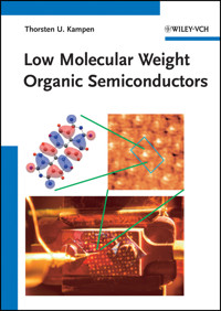
This up-to-date reference for students and researchers in the field is the first systematic treatment on the property measurements of organic semiconductor materials. Following an introduction, the book goes on to treat the structural analysis of thin films and spectroscopy of electronic states. Subsequent sections deal with optical spectroscopy and charge transport. An invaluable source for understanding, handling and applying this key type of material for physicists, materials scientists, graduate students, and analytical laboratories.
Sie lesen das E-Book in den Legimi-Apps auf:
Seitenzahl: 278
Veröffentlichungsjahr: 2011
Ähnliche
Contents
Preface
1 Introduction
1.1 Electronic Surface Properties of Inorganic Semiconductors
1.2 Semiconductor Interfaces
2 Growth of Thin Films
2.1 Purification
2.2 Organic Molecular Beam Deposition
2.3 Organic Vapor Phase Deposition
3 Structural Analysis
3.1 Scanning Probe Microscopy
3.2 X-Ray Diffraction (XRD)
3.3 Low-Energy Electron Diffraction
4 Optical Spectroscopy
4.1 Photoluminescence
4.2 Raman Spectroscopy
4.3 Infrared Spectroscopy
4.4 Ellipsometry
4.5 Reflection Anisotropy Spectroscopy
5 Electronic and Chemical Surface Properties
5.1 Photoemission Spectroscopy
5.2 Inverse Photoemission
5.3 Total Current Spectroscopy
5.4 Near Edge X-ray Absorption Fine Structure Spectroscopy
6 Charge Transport
6.1 Time-of-flight measurements (TOF)
6.2 Thin Field Effect Transistor (TFT) Mobilities
6.3 I/V Curves of Ag/GaAs(100) Schottky Contacts
6.4 Charge Carrier Mobilities
6.5 Simulation of IV Curves
6.6 Chemical Stability
6.7 Deep level transient spectroscopy
6.8 Organic-Modified Schottky Diodes for Frequency Mixer Applications
References
Index
Related Titles
Yersin, H. (ed.)Highly Efficient OLEDs with Phosphorescent Materials458 pages with approx.195 figures and approx. 40 tables2008HardcoverISBN: 978-3-527-40594-7
Hadziioannou, G., Malliaras, G. G. (eds.)Semiconducting PolymersChemistry, Physics and Engineering768 pages in 2 volumeswith 402 figures and 3 tables2007HardcoverISBN: 978-3-527-31271-9
Klauk, H. (ed.)Organic ElectronicsMaterials, Manufacturing and Applications446 pages with 281 figures and 21 tables2006HardcoverISBN: 978-3-527-31264-1
Müllen, K., Scherf, U. (eds.)Organic Light Emitting DevicesSynthesis, Properties and Applications426 pages with 258 figures and 14 tables2006HardcoverISBN: 978-3-527-31218-4
Brütting, W. (ed.)Physics of Organic Semiconductors554 pages with 323 figures2005HardcoverISBN: 978-3-527-40550-3
The Author
PD Dr.rer.nat. Thorsten U. KampenSPECS GmbH, Berlin, GermanyTU Berlin, Germany
All books published by Wiley-VCH are carefully produced. Nevertheless, authors, editors, and publisher do not warrant the information contained in these books, including this book, to be free of errors. Readers are advised to keep in mind that statements, data, illustrations, procedural details or other items may inadvertently be inaccurate.
Library of Congress Card No.:applied for
British Library Cataloguing-in-Publication DataA catalogue record for this book is available from the British Library.
Bibliographic information published by the Deutsche NationalbibliothekThe Deutsche Nationalbibliothek lists this publication in the Deutsche Nationalbibliografie; detailed bibliographic data are available on the Internet at http://dnb.d-nb.de.
© 2010 WILEY-VCH Verlag GmbH & Co. KGaA, Weinheim
All rights reserved (including those of translation into other languages). No part of this book may be reproduced in any form – by photoprinting, microfilm, or any other means – nor transmitted or translated into a machine language without written permission from the publishers.Registered names, trademarks, etc. used in this book, even when not specifically marked as such, are not to be considered unprotected by law.
Cover Design Adam-Design, Weinheim
ISBN: 978-3-527-40653-1
Preface
This book has covers the physical properties of organic and their application in organic/inorganic interfaces. The investigations have been performed using complementary experimental and theoretical techniques. Here, the collaborations within the European Research Training Network known as DIODE (Designing Inorganic Organic Devices, HPRN-CT-1999-00164) have played an important role.
In this respect, I have to thank Iggy McGovern, Justin Wells, and Gregory Cabailh from the Trinity College in Dublin, Ireland, as well as Andrew Evans, Alex Veary-Roberts, and Adam Bushell from the University of Wales in Aberystwyth for their cooperation during synchrotron beamtimes at BESSY I and II in Berlin. Javier Mendez from Universidad Autonoma de Madrid, Spain, performed the atomic force microscopy investigations shown in this work. Concerning the theoretical part of this work, I have to thank Fernando Flores from the Universidad Autonoma de Madrid for a long and fruitful cooperation in the field of semiconductor surfaces and interfaces. The simulations of the current-voltage characteristics of organic modified Schottky contacts have been done in collaboration with Aldo DiCarlo from Universita degli Studi di Roma “Tor Vergata “in Italy.
I want to thank Walter Braun, Torsten Kachel, Patrick Bressler, and David Batchelor from BESSY in Berlin, Germany, for their support during our synchrotron beamtimes. The research at this facility was funded by the Bundesministerium für Bildung und Forschung in Germany (BMBF contract No. 05 KS1OCA/1).
Thanks are due to Norbert Karl (University of Stuttgart, Germany) and Antoine Kahn (Princeton University, USA) for long and intense discussions on the properties of organic semiconductors and their interfaces.
I had a wonderful and exciting time during my stay at the University of Nagoya, Japan, in 2000. Kazuhiko Seki and Hisao Ishii took care of me in every aspect, and since then, the research groups in Nagoya and Chemnitz have a fruitful collaboration in vibrational spectroscopy investigations on organic/metal interfaces.
My special thanks go to the former and momentary members of the Semiconductor Physics group at Chemnitz University of Technology. I am indebted to: Arindam Das, Kornelia Dostmann, Axel Fechner, Marion Friedrich, Gianina Gavrila, Pham Truong Giang, Mihaela Gorgoi, Cameliu Himcinschi, Stefan Hohenecker, Andrei Kobitski, Martin Lübbe, Thomas Lindner, Henry Mendez, Andreea Paraian, Sunggook Park, Sybille Raschke, Georgeta Salvan, Dmitri Tenne, and Ilja Thurzo.
Wolfram Fliegel from Freiberger Compound Materials GmbH in Freiberg, Germany, supplied GaAs wafers.
Since I started working with organic materials, Reinhard Scholz (TU Muenchen Germany) has been always a willing confidant when discussing all aspects of the physical properties of organic materials. I am especially indebted to Dietrich R. T. Zahn for giving me the opportunity to work in his group.
That I was able to complete this work at all is a tribute to my beloved wife Ellen, who inspired and goaded me into keeping up the work. I have to thank her for her patience and never ending support.
My scientific approach to organic semiconductors is based on my scientific background before I started working in this field, that is, semiconductor surfaces and interfaces. This and the outline of research in the above mentioned DIODE network determines the outline of this book. In the DIODE network we focused on the modification of metal semiconductor interfaces using organic molecules. We had the unique opportunity to start from basic research on finding the proper prepared semiconductor surface for organic growth, then investigating the bulk and interface properties of the organic films grown on inorganic semiconductor substrates, and finally using the findings to optimise and test a real device.
Therefore, the book starts with an introduction into the surface and interface properties of inorganic semiconductor surface in Chapter 1. Chapter 2 and 3 present the techniques for the purification/growth of organic semiconductors and the resulting structural properties, respectively. The optical properties of such thin films are presented in Chapter 4, while Chapter 5 discusses the chemical and electronic surface properties. Finally, Chapter 6 presents charge transport properties. The experimental results presented are obtained with a variety of complementary techniques which are briefly introduced.
Thorsten U. Kampen
1
Introduction
The reports of efficient electroluminescence from conjugated polymers [1] and small molecules [2] have triggered spectacular developments in the field of organic-based electro-optic and electronic devices, such as optical switches [3], batteries [4], field-effect transistors and circuits [5, 6], identification and product tagging [5, 7], data storage and computing [8], sensors and actuators [9], solar cells [10], organic light-emitting diodes (OLEDs) [1], flat panel displays [11, 12], photodiodes, solar cells, solid-state lasers, integrated circuits, and waveguides [13–15]. The low synthesis costs and relative easiness of handling make this new class of materials attractive for the above-mentioned applications. Furthermore, the chemical compatibility of organic materials with plastics allows the low-cost fabrication of flexible, unbreakable, and transparent devices.
However, the low mobility of organic semiconductors precludes the complete replacement of compound inorganic materials, especially for high-frequency applications. On the other hand, organic semiconductor can be used in hybrid organic/inorganic devices to tailor properties and performances of conventional high -frequency devices. One of the possible applications of ultrathin layers of organic molecules is the passivation of semiconductor surfaces, such as Si(111)-(7 × 7) and GaAs(100) [16]. For example, a C 60 monolayer on a Si(111)-(7 × 7) surface inhibits chemical contamination by water and atmospheric oxygen.
Another application is the organic modification of metal–semiconductor or Schottky contacts. Schottky diodes are often used for mixing applications in telecommunication systems, radio astronomy, radar technology, and plasma diagnostics [17]. One disadvantage is the relatively high bias voltage necessary to operate mixer diodes. This leads to high power consumption or low sensitivities combined with high requirements concerning the stability and noise of the voltage sources.
Lesen Sie weiter in der vollständigen Ausgabe!
Lesen Sie weiter in der vollständigen Ausgabe!
Lesen Sie weiter in der vollständigen Ausgabe!
Lesen Sie weiter in der vollständigen Ausgabe!
Lesen Sie weiter in der vollständigen Ausgabe!
Lesen Sie weiter in der vollständigen Ausgabe!
Lesen Sie weiter in der vollständigen Ausgabe!


