Molecular Beam Epitaxy E-Book
189,99 €
Mehr erfahren.
- Herausgeber: John Wiley & Sons
- Kategorie: Fachliteratur
- Serie: Wiley Series in Materials for Electronic & Optoelectronic Applications
- Sprache: Englisch
Covers both the fundamentals and the state-of-the-art technology used for MBE
Written by expert researchers working on the frontlines of the field, this book covers fundamentals of Molecular Beam Epitaxy (MBE) technology and science, as well as state-of-the-art MBE technology for electronic and optoelectronic device applications. MBE applications to magnetic semiconductor materials are also included for future magnetic and spintronic device applications.
Molecular Beam Epitaxy: Materials and Applications for Electronics and Optoelectronics is presented in five parts: Fundamentals of MBE; MBE technology for electronic devices application; MBE for optoelectronic devices; Magnetic semiconductors and spintronics devices; and Challenge of MBE to new materials and new researches. The book offers chapters covering the history of MBE; principles of MBE and fundamental mechanism of MBE growth; migration enhanced epitaxy and its application; quantum dot formation and selective area growth by MBE; MBE of III-nitride semiconductors for electronic devices; MBE for Tunnel-FETs; applications of III-V semiconductor quantum dots in optoelectronic devices; MBE of III-V and III-nitride heterostructures for optoelectronic devices with emission wavelengths from THz to ultraviolet; MBE of III-V semiconductors for mid-infrared photodetectors and solar cells; dilute magnetic semiconductor materials and ferromagnet/semiconductor heterostructures and their application to spintronic devices; applications of bismuth-containing III–V semiconductors in devices; MBE growth and device applications of Ga2O3; Heterovalent semiconductor structures and their device applications; and more.
- Includes chapters on the fundamentals of MBE
- Covers new challenging researches in MBE and new technologies
- Edited by two pioneers in the field of MBE with contributions from well-known MBE authors including three Al Cho MBE Award winners
- Part of the Materials for Electronic and Optoelectronic Applications series
Molecular Beam Epitaxy: Materials and Applications for Electronics and Optoelectronics will appeal to graduate students, researchers in academia and industry, and others interested in the area of epitaxial growth.
Sie lesen das E-Book in den Legimi-Apps auf:
Seitenzahl: 998
Veröffentlichungsjahr: 2019
Ähnliche


Wiley Series in Materials for Electronic & Optoelectronic Applications
www.wiley.com/go/meoa
Series Editors
Professor Arthur Willoughby, University of Southampton, Southampton, UK
Dr Peter Capper, SELEX Galileo Infrared Ltd, Southampton, UK
Professor Safa Kasap, University of Saskatchewan, Saskatoon, Canada
Published Titles
Bulk Crystal Growth of Electronic, Optical and Optoelectronic Materials, Edited by P. Capper
Properties of Group‐IV, III–V and II–VI Semiconductors, S. Adachi
Charge Transport in Disordered Solids with Applications in Electronics, Edited by S. Baranovski
Optical Properties of Condensed Matter and Applications, Edited by J. Singh
Thin Film Solar Cells: Fabrication, Characterization, and Applications, Edited by J. Poortmans and V. Arkhipov
Dielectric Films for Advanced Microelectronics, Edited by M. R. Baklanov, M. Green, and K. Maex
Liquid Phase Epitaxy of Electronic, Optical and Optoelectronic Materials, Edited by P. Capper and M. Mauk
Molecular Electronics: From Principles to Practice, M. Petty
CVD Diamond for Electronic Devices and Sensors, Edited by R. S. Sussmann
Properties of Semiconductor Alloys: Group‐IV, III–V, and II–VI Semiconductors, S. Adachi
Mercury Cadmium Telluride, Edited by P. Capper and J. Garland
Zinc Oxide Materials for Electronic and Optoelectronic Device Applications, Edited by C. Litton,
D. C. Reynolds, and T. C. Collins
Lead‐Free Solders: Materials Reliability for Electronics, Edited by K. N. Subramanian
Silicon Photonics: Fundamentals and Devices, M. Jamal Deen and P. K. Basu
Nanostructured and Subwavelength Waveguides: Fundamentals and Applications, M. Skorobogatiy
Photovoltaic Materials: From Crystalline Silicon to Third‐Generation Approaches, Edited by G. Conibeer and A. Willoughby
Glancing Angle Deposition of Thin Films: Engineering the Nanoscale, Matthew M. Hawkeye,
Michael T. Taschuk, and Michael J. Brett
Physical Properties of High‐Temperature Superconductors, R. Wesche
Spintronics for Next Generation Innovative Devices, Edited by Katsuaki Sato, Eiji Saitoh
Inorganic Glasses for Photonics: Fundamentals, Engineering and Applications, Animesh Jha
Amorphous Semiconductors: Structural, Optical and Electronic Properties, Kazuo Morigaki, Sandor Kugler, Koichi Shimakawa
Microwave Materials and Applications 2 Vol set, Edited by Mailadil T. Sebastian, Rick Ubic, Heli Jantunen
Molecular Beam Epitaxy
Materials and Applications for Electronics and Optoelectronics
Edited by
HAJIME ASAHI
ISIR, Osaka University, Japan
YOSHIJI HORIKOSHI
Waseda University, Tokyo, Japan
Copyright
This edition first published 2019
© 2019 John Wiley & Sons Ltd
All rights reserved. No part of this publication may be reproduced, stored in a retrieval system, or transmitted, in any form or by any means, electronic, mechanical, photocopying, recording or otherwise, except as permitted by law. Advice on how to obtain permission to reuse material from this title is available at http://www.wiley.com/go/permissions.
The right of Hajime Asahi and Yoshiji Horikoshi to be identified as the authors of the editorial material in this work has been asserted in accordance with law.
Registered Offices
John Wiley & Sons, Inc., 111 River Street, Hoboken, NJ 07030, USA
John Wiley & Sons Ltd, The Atrium, Southern Gate, Chichester, West Sussex, PO19 8SQ, UK
Editorial Office
The Atrium, Southern Gate, Chichester, West Sussex, PO19 8SQ, UK
For details of our global editorial offices, customer services, and more information about Wiley products visit us at www.wiley.com.
Wiley also publishes its books in a variety of electronic formats and by print‐on‐demand. Some content that appears in standard print versions of this book may not be available in other formats.
Limit of Liability/Disclaimer of Warranty
In view of ongoing research, equipment modifications, changes in governmental regulations, and the constant flow of information relating to the use of experimental reagents, equipment, and devices, the reader is urged to review and evaluate the information provided in the package insert or instructions for each chemical, piece of equipment, reagent, or device for, among other things, any changes in the instructions or indication of usage and for added warnings and precautions. While the publisher and authors have used their best efforts in preparing this work, they make no representations or warranties with respect to the accuracy or completeness of the contents of this work and specifically disclaim all warranties, including without limitation any implied warranties of merchantability or fitness for a particular purpose. No warranty may be created or extended by sales representatives, written sales materials or promotional statements for this work. The fact that an organization, website, or product is referred to in this work as a citation and/or potential source of further information does not mean that the publisher and authors endorse the information or services the organization, website, or product may provide or recommendations it may make. This work is sold with the understanding that the publisher is not engaged in rendering professional services. The advice and strategies contained herein may not be suitable for your situation. You should consult with a specialist where appropriate. Further, readers should be aware that websites listed in this work may have changed or disappeared between when this work was written and when it is read. Neither the publisher nor authors shall be liable for any loss of profit or any other commercial damages, including but not limited to special, incidental, consequential, or other damages.
Library of Congress Cataloging‐in‐Publication Data
Names: Asahi, Hajime, 1948‐ editor. | Horikoshi, Yoshiji, 1943‐ editor.
Title: Molecular beam epitaxy : materials and applications for electronics
and optoelectronics / edited by Hajime Asahi (ISIR, Osaka University,
Japan), Yoshiji Horikoshi (Waseda University, Tokyo, Japan).
Description: First edition. | Hoboken, NJ : Wiley, 2019. | Series: Wiley
series in materials for electronic & optoelectronic applications |
Includes bibliographical references and index. |
Identifiers: LCCN 2018044564 (print) | LCCN 2018059153 (ebook) | ISBN
9781119355007 (Adobe PDF) | ISBN 9781119355021 (ePub) | ISBN 9781119355014
(hardcover)
Subjects: LCSH: Molecular beam epitaxy. | Epitaxy. | Crystal growth. |
Electronics–Materials. | Optoelectronics–Materials.
Classification: LCC QC611.6.M64 (ebook) | LCC QC611.6.M64 M6455 2019 (print)
| DDC 621.3815/2–dc23
LC record available at https://lccn.loc.gov/2018044564
Cover Design: Dan Jubb
Cover Images: Courtesy of Yoshiji Horikoshi
List of Contributors
Rolf J. Aidam, Fraunhofer Institute for Applied Solid State Physics, Germany
Kouichi Akahane, National Institute of Information and Communication Technology, Japan
O. Ambacher, Fraunhofer Institute for Applied Solid State Physics, Germany
Hajime Asahi, The Institute of Scientific and Industrial Research, Osaka University, Japan
Harvey E. Beere, Department of Physics, Cavendish Laboratory, University of Cambridge, UK
Pallab Bhattacharya, Department of Electrical Engineering and Computer Science, University of Michigan, USA
Saniya Deshpande, Department of Electrical Engineering and Computer Science, University of Michigan, USA
E. Diwo, Fraunhofer Institute for Applied Solid State Physics, Germany
A. Feduniewicz‐Żmuda, Institute of High Pressure Physics, Polish Academy of Sciences, Poland
Xiao Feng, Tsinghua University, Beijing, China
Micha N. Fireman, University of Carifornia, Santa Barbara, USA
Tom Foxon, Nottingham University, UK
Thomas Frost, Department of Electrical Engineering and Computer Science, University of Michigan, USA
B.‐J. Godejohann, Fraunhofer Institute for Applied Solid State Physics, Germany
Arnab Hazari, Department of Electrical Engineering and Computer Science, University of Michigan, USA
Ke He, Tsinghua University, Beijing, China
Masataka Higashiwaki, National Institute of Information and Communications Technology, Tokyo, Japan
Yoshiji Horikoshi, Waseda University, Tokyo, Japan
Shafat Jahangir, Department of Electrical Engineering and Computer Science, University of Michigan, USA
Bharat Jalan, University of Minnesota, USA
Yuichi Kawamura, Osaka Prefecture University, Japan
Salim El Kazzi, Interuniversity Microelectronics Center, Belgium
L. Kirste, Fraunhofer Institute for Applied Solid State Physics, Germany
Katsumi Kishino, Sophia University, Tokyo, Japan
Philip C. Klipstein, SemiConductor Devices, Israel
Shinji Kuroda, Institute of Materials Science, University of Tsukuba, Japan
T. Lim, Fraunhofer Institute for Applied Solid State Physics, Germany
J. Marcelo J. Lopes, Paul‐Drude‐Institut für Festkörperelektronik, Berlin, Germany
Xucun Ma, Tsinghua University, Beijing, China
Hiro Munekata, Tokyo Institute of Technology, Japan
G. Muziol, Institute of High Pressure Physics, Polish Academy of Sciences, Poland
Yoshiaki Nakata, National Institute of Information and Communication Technology, Japan
Tianxiao Nie, Fert Beijing Institute, BDBC, and School of Electronic and Information Engineering, Beihang University, China and Device Research Laboratory, Department of Electrical Engineering, University of California, USA
K. Nowakowski‐Szkudlarek, Institute of High Pressure Physics, Polish Academy of Sciences, Poland
Abhinav Prakash, University of Minnesota, USA
R. Quay, Fraunhofer Institute for Applied Solid State Physics, Germany
David. A. Ritchie, Department of Physics, Cavendish Laboratory, University of Cambridge, UK
Marta Sawicka, Institute of High Pressure Physics, Polish Academy of Sciences, Poland and TopGaN Ltd., Poland
M. Siekacz, Institute of High Pressure Physics, Polish Academy of Sciences, Poland
Czeslaw Skierbiszewski, Institute of High Pressure Physics, Polish Academy of Sciences, Poland and TopGaN Ltd., Poland
James S. Speck, University of California, Santa Barbara, USA
Takeyoshi Sugaya, National Institute of Advanced Industrial Science and Technology, Japan
Masaaki Tanaka, Center for Spintronics Research Network, and Department of Electrical Engineering & Information Systems, and Institute for Nano Quantum Information Electronics, University of Tokyo, Japan
Jianshi Tang, IBM Thomas J. Watson Research Center, USA
Eric Tournie, IES, Université de Montpellier, France
Shiro Tsukamoto, National Institute of Technology, Anan College, Japan
H. Turski, Institute of High Pressure Physics, Polish Academy of Sciences, Poland
P. Waltereit, Fraunhofer Institute for Applied Solid State Physics, Germany
Kang L. Wang, Device Research Laboratory, Department of Electrical Engineering, University of California, USA
P. Wolny, Institute of High Pressure Physics, Polish Academy of Sciences, Poland
Qi‐Kun Xue, Tsinghua University, Beijing, China
Koichi Yamaguchi, The University of Electro‐Communications, Tokyo, Japan
Masahiro Yoshimoto, Kyoto Institute of Technology, Kyoto, Japan
Yong‐Hang Zhang, Arizona State University, Arizona, USA
Yi‐Kai Zhou, The Institute of Scientific and Industrial Research, Osaka University, Japan and Key Laboratory of Optoelectronic Material and Device, Mathematics & Science College, Shanghai Normal University, China
Series Preface
Wiley Series in Materials for Electronic and Optoelectronic Applications
This book series is devoted to the rapidly developing class of materials used for electronic and optoelectronic applications. It is designed to provide much‐needed information on the fundamental scientific principles of these materials, together with how these are employed in technological applications. The books are aimed at (postgraduate) students, researchers and technologists, engaged in research, development and the study of materials in electronics and photonics, and industrial scientists developing new materials, devices and circuits for the electronic, optoelectronic and communications industries.
The development of new electronic and optoelectronic materials depends not only on materials engineering at a practical level, but also on a clear understanding of the properties of materials, and the fundamental science behind these properties. It is the properties of a material that eventually determine its usefulness in an application. The series therefore also includes such titles as electrical conduction in solids, optical properties, thermal properties, and so on, all with applications and examples of materials in electronics and optoelectronics. The characterization of materials is also covered within the series in as much as it is impossible to develop new materials without the proper characterization of their structure and properties. Structure‐property relationships have always been fundamentally and intrinsically important to materials science and engineering.
Materials science is well known for being one of the most interdisciplinary sciences. It is the interdisciplinary aspect of materials science that has led to many exciting discoveries, new materials and new applications. It is not unusual to find scientists with a chemical engineering background working on materials projects with applications in electronics. In selecting titles for the series, we have tried to maintain the interdisciplinary aspect of the field, and hence its excitement to researchers in this field.
Arthur Willoughby
Peter Capper
Safa Kasap
Preface
More than 50 years have passed since the first epitaxial growth of semiconductors was recognized by molecular beam epitaxy (MBE). During these decades, tremendous improvements have been made in the MBE apparatus itself and in‐situ evaluation methods. These improvements are directly connected to the quality of grown materials and devices created from them. Indeed, many brilliant results have been achieved, such as quantum well lasers, quantum cascade lasers, high electron mobility materials exceeding 107 cm2 V−1 s−1, to name but a few. Even now, these efforts are ongoing, and MBE therefore still attracts many researchers for investigations on new materials and new device applications.
In the last few decades, many books have been published on MBE related topics. Our book is distinguished from these by discussion not only of the fundamentals and state of the art of MBE technology, but also by discussion of new challenging research. We hope that this book will encourage young researchers and students to explore new fields of research and applications.
This book covers the fundamentals of MBE technology and science, and state‐of‐the‐art MBE technology for electronic and optoelectronic device applications. MBE research on magnetic semiconductor materials is also included for future magnetic and spintronic device applications. The book consists of the following five parts: I, Fundamentals of MBE; II, MBE Technology for Electronic Devices Application; III, MBE for Optoelectronic Devices; IV, Magnetic Semiconductors and Spintronics Devices; V, Challenge of MBE to New Materials and New Researches. There are twenty‐eight chapters divided between the five parts, all written by researchers working actively in the front line.
Part I starts with an overview of the history of MBE, from the early stages of MBE technology to modern advanced MBE technology, and the principles of MBE and fundamental mechanisms of MBE growth are described. It also includes migration‐enhanced epitaxy (MEE), which helps in understanding the atomic processes of MBE. Quantum dot formation through self‐assembly processes and low‐dimensional structures by selective area epitaxy are also discussed. In Part II, MBE of III‐nitride semiconductors for electronic devices and application of MBE to electronic devices using the tunneling effect are described. Part III covers MBE for the light emitters of various semiconductors (III–V and III‐nitrides) with emission wavelengths in the range from terahertz to ultraviolet. MBE growth of the materials for mid‐infrared photodetectors and solar cells is also described. Part IV covers MBE growth for dilute magnetic semiconductor materials and their application to spintronic devices based on III–V, III‐nitrides, II–VI, and IV. MBE growth of ferromagnet/semiconductor heterostructures is also described for spintronic applications. Recent new challenges in MBE research are collected in Part V. MBE is a versatile growth technique for creating high‐quality materials and devices, and has great potential in opening up new material and fundamental researches.
Part IFundamentals of MBE
1History of MBE
Tom Foxon
Department of Physics and Astronomy, Nottingham University, Nottingham, NG7 2RD, UK
1.1 Introduction
John Orton and I have recently published a book entitled Molecular Beam Epitaxy – A Short History[1]. In that book we were not able to cover all aspects of this topic, so many significant contributions had to be omitted. In this short chapter, even more work of importance will be missing and what follows is my personal view of how molecular beam epitaxy (MBE) evolved. Before starting to describe how it occurred, we have of course to decide what we mean by MBE. As far as I can discover, the term was first used in the Proceedings of the Third International Symposium on GaAs and Related Compounds by Cho et al. [2] in order to distinguish MBE from the earlier growth methods, namely liquid phase epitaxy (LPE) and vapour phase epitaxy (VPE). So, what is MBE? One may consider it to be a refined form of vacuum evaporation, but it is clearly significantly different from simple evaporation in many ways. It usually involves multiple sources and deposition onto a heated substrate. It usually takes place in ultra‐high vacuum (UHV) equipment, in order to reduce the arrival rate of unwanted species. In general, collision‐free molecular beams are used to supply the required species to the substrate. It differs from many other growth methods in having many different in‐situ measurements (e.g. electron diffraction or mass spectrometry), which enables the process to be controlled at an atomic level. My personal view is that there are at least two MBE topics of equal importance, there is the study of the MBE process itself and the application of MBE to provide samples and devices of the highest possible quality. In my career I have been involved in both aspects for a variety of material systems and regard them as equally significant. In this chapter I will try to summarise what went into our book and will begin by discussing the development of the MBE process before turning to its application. Before starting on this task, I recommend to the reader two review articles published by three of the pioneers of MBE in 1974 [3] and 1975 [4], respectively. The first deals with epitaxy in general, whilst the second deals exclusively with MBE and gives a comprehensive account of the state of the art at that time (1975).
In what follows I will try to avoid too much overlap with the following chapters, so comments on devices, magnetic semiconductors and new materials will be very brief.
1.2 The MBE Process
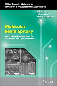
As far as I am aware, the first studies of growth, by what we now call MBE, were performed at Plessey Labs in Caswell by Bruce Joyce and co‐workers. They grew Si films from molecular beams of silane on a heated Si substrate under UHV conditions and the resulting samples were studied by Roger Booker at Cambridge University using transmission electron microscopy (TEM). This study was concerned with the nucleation process itself and very low growth rates were used in order to separate reactions on the surface from those in the gas phase, hence the need for collision‐free molecular beams. This work was published in a series of papers from 1966 onwards [5–7] and was summarised in a review article by Bruce Joyce in 1968 [8]. The equipment used for this study had many of the attributes of a modern MBE system (having collimated, collision‐free, molecular beams of silane impinging on a heated Si substrate) and took place under UHV conditions; the pressure during growth in the reaction chamber was ∼3 × 10⁻⁹ Torr. The growth rates were small compared to modern practise and no in‐situ characterisation was involved, but in all other respects this could be considered to be the first study of the MBE growth process. A result from this study is shown in Figure 1.1, where it is clear that Si grows epitaxially on the heated Si substrate by decomposition from the molecular beam of silane [8], in other words by MBE.
Figure 1.1 MBE deposition of Si from silane on a heated Si substrate under UHV conditions [8].
Following this initial work on Si, what followed was the use of MBE to grow compound semiconductors, mainly III–Vs and to a lesser extent II–VIs, motivated in part by the desire to produce semiconductor lasers. The initial work on lasers was carried out using LPE (for those interested in the development of solid‐state lasers, see the excellent book on the story of semiconductors [9]), but it soon became apparent that MBE could produce equivalent or better results. What followed was the development of MBE for many practical device applications, including lasers, transistors, and so on.
Shortly after the work at Plessey came the pioneering work at Bell Labs by John Arthur and co‐workers, who studied the interaction of molecular beams of gallium and arsenic on a heated GaAs substrate using in‐situ mass spectrometry [10]. This was followed by a study of the growth of GaAs, GaP and GaAsP by what he termed molecular beam deposition [11]. In his system the sources were surrounded by a liquid nitrogen‐cooled shroud and in‐situ mass spectrometry, Auger electron spectroscopy (AES) and low‐energy electron diffraction (LEED) were used for in‐situ analysis. The system also had provision for cleaning the substrate prior to growth using an argon ion gun. The mass spectrometer could be rotated to enable it to measure either the beams from the Knudsen cells or the species desorbing from the surface. From this study it became clear that for III–Vs the growth rate is controlled by the arrival rate of the group III species, providing there is an excess of the group V species. It also showed that the relative sticking coefficients for As and P are very different.
Shortly after Arthur's work at Bell Labs, Al Cho joined Morton B. Panish's group and embarked on his pioneering study of MBE. As everyone knows, he made outstanding contributions to both understanding the MBE process and its practical application for devices. His system had a reflection high‐energy electron diffraction (RHEED) system for surface analysis, an argon ion gun for surface cleaning, a cylindrical mirror analysis Auger system for surface composition and again the cells were mounted within a liquid nitrogen‐cooled shroud. The change from LEED to RHEED was crucial and enabled real‐time surface analysis, which has become the de‐facto standard in all modern MBE systems. I will discuss Al Cho's many contributions to the growth of structures for low‐dimensional structures and devices below, but here I wish to point out some of his critical contributions to understanding the MBE process. One of his most important contributions was to show, using RHEED, that for both the (111) [12] and (001) [13] surfaces a clear correlation exists between the surface structure we observe and both the III–V ratio and substrate temperature. The second paper [13] established the fact that under As‐rich conditions on the (001) surface we see a c(2 × 8) RHEED pattern, which becomes a c(8 × 2) pattern under Ga‐rich conditions; in between we also see other 6× patterns. This crucial observation enabled others to follow the process and establish the optimum III–V ratio and substrate temperature for growth. In 1971 he also published a paper showing how the RHEED pattern develops during growth from diffuse spots to streaks and at the same time the surface goes from rough to smooth [14]. This work was done long before atomic resolution of the surface by atomic force microscopy (AFM


