111,99 €
Mehr erfahren.
- Herausgeber: Wiley-VCH
- Kategorie: Wissenschaft und neue Technologien
- Sprache: Englisch
The International System of Units (SI) is the world's most widely used system of measurement, used every day in commerce and science, and is the modern form of the metric system. It currently comprises the meter (m), the kilogram (kg), the second (s), the ampere (A), the kelvin (K), the candela (cd) and the mole (mol)). The system is changing though, units and unit definitions are modified through international agreements as the technology of measurement progresses, and as the precision of measurements improves. The SI is now being redefined based on constants of nature and their realization by quantum standards. Therefore, the underlying physics and technologies will receive increasing interest, and not only in the metrology community but in all fields of science.
This book introduces and explains the applications of modern physics concepts to metrology, the science and the applications of measurements. A special focus is made on the use of quantum standards for the realization of the forthcoming new SI (the international system of units). The basic physical phenomena are introduced on a level which provides comprehensive information for the experienced reader but also provides a guide for a more intense study of these phenomena for students.
Sie lesen das E-Book in den Legimi-Apps auf:
Seitenzahl: 448
Veröffentlichungsjahr: 2015
Ähnliche


Table of Contents
Cover
Related Titles
Title Page
Copyright
Foreword
Preface
List of Abbreviations
Chapter 1: Introduction
References
Chapter 2: Some Basics
2.1 Measurement
2.2 The SI (Système International d'Unités)
References
Chapter 3: Laser Cooling, Atomic Clocks, and the Second
3.1 Techniques for Laser Cooling
3.2 The Cs Fountain Clock
3.3 Optical Clocks
References
Chapter 4: Superconductivity, Josephson Effect, and Flux Quanta
4.1 Josephson Effect and Quantum Voltage Standards
4.2 Flux Quanta and SQUIDs
References
Chapter 5: Quantum Hall Effect
5.1 Basic Physics of Three- and Two-Dimensional Semiconductors
5.2 Two-Dimensional Electron Systems in Real Semiconductors
5.3 The Hall Effect
5.4 Quantum Hall Resistance Standards
References
Chapter 6: Single-Charge Transfer Devices and the New Ampere
6.1 Basic Physics of Single-Electron Transport
6.2 Quantized Current Sources
6.3 Consistency Tests: Quantum Metrology Triangle
References
Chapter 7: The Planck Constant, the New Kilogram, and the Mole
7.1 The Avogadro Experiment
7.2 The Watt Balance Experiment
7.3 The Mole: Unit of Amount of Substance
References
Chapter 8: Boltzmann Constant and the New Kelvin
8.1 Primary Thermometers
8.2 Realization and Dissemination of the New Kelvin
References
Chapter 9: Single-Photon Metrology and Quantum Radiometry
9.1 Single-Photon Sources
9.2 Single-Photon Detectors
9.3 Metrological Challenge
References
Chapter 10: Outlook
References
Index
End User License Agreement
Pages
ix
x
xi
xii
xiii
xiv
xv
1
2
3
5
6
7
8
9
10
11
12
13
14
15
16
17
18
19
20
21
22
23
24
25
26
27
28
29
30
31
32
33
34
35
36
37
38
39
40
41
42
43
44
45
46
47
48
49
50
51
52
53
54
55
56
57
58
59
61
62
63
64
65
66
67
68
69
70
71
72
73
74
75
76
77
78
79
80
81
82
83
84
85
86
87
88
89
90
91
92
93
94
95
96
97
98
99
100
101
102
103
104
105
106
107
108
109
110
111
112
113
114
115
116
117
118
119
120
121
122
123
124
125
126
127
128
131
132
133
134
135
136
137
138
139
140
141
142
143
144
145
146
147
148
149
150
151
152
153
154
155
156
157
158
159
160
161
162
163
164
165
166
167
168
169
170
171
172
173
175
176
177
178
179
180
181
182
183
184
185
186
187
188
189
191
192
193
194
195
196
197
198
199
200
201
202
203
204
205
207
208
209
210
211
Guide
Cover
Table of Contents
Foreword
Preface
Begin Reading
List of Illustrations
Chapter 2: Some Basics
Figure 2.1 Components and quantities considered (left) and the minimum current,
I
min
, and the minimum magnetic flux, Φ
min
, versus inductance,
L
, for an ideal coil.
Figure 2.2 Noise power spectral density,
P
(
T
,
f
), versus frequency for different temperatures.
Figure 2.3 Noise power spectral density as measured for a SQUID magnetometer versus frequency.
Figure 2.4 Schematic representation of a “thermal” Cs atomic clock. In the lower left a section of a Ramsey resonance curve is shown.
I
D
is the current of the ionization detector.
Figure 2.5 Measured Ramsey fringe pattern for the PTB's CS1 thermal-beam clock. The curve appears upside down compared to the result of Eq. (2.19) due to the special operation configuration of PTB CS1.
Figure 2.6 The Pt/Ir kilogram prototype as stored at the
Bureau International des Poids et Mesures
(BIPM).
Chapter 3: Laser Cooling, Atomic Clocks, and the Second
Figure 3.9 Energy level scheme of the lower states in
133
Cs.
Figure 3.1 Laser beam arrangement for an optical molasses.
Figure 3.2 Energy levels and laser beam arrangement in a (1D) MOT.
Figure 3.3 Illustration of Sisyphus cooling. (a) The polarization along the
z
direction in a “lin lin” standing wave configuration. (b) The corresponding light shift of the and ground state. (From [2], with kind permission from Wiley-VCH.)
Figure 3.4 Potential landscape of a two-dimensional optical lattice.
Figure 3.5 Two-dimensional sectional view of the electrode configuration and electric field distribution (for two half cycles of the rf field) of a three-dimensional Paul trap. The arrows labelled
E
and
F
E
denote the resulting instantaneous electric field and force, respectively.
Figure 3.6 Configuration of linear Paul traps with additional ring electrodes (a) or seqmented rods (b) for axial confinement.
Figure 3.7 Yb
+
ions (seen by their fluorescence) in a linear Paul trap. The distance between the ions is about 10–20 µm. (Courtesy of T. Mehlstäubler, PTB.)
Figure 3.8 Schematic setup (simplified) of an atomic fountain clock.
Figure 3.10 Principle of operation of the atomic fountain clock illustrating the essential four steps in a measurement cycle: (a) preparation of the cloud of cold atoms, (b) launch of the cloud toward the microwave cavity and subsequent passage through the state selection cavity and Ramsey cavity, (c) free flight and turnaround of the cloud and subsequent second passage through the Ramsey cavity, and (d) detection of the number of atoms in the and states, respectively. (Courtesy of R. Wynands, PTB.)
Figure 3.11 Principle of operation of an optical clock.
Figure 3.12 Scheme of a Bordé–Ramsey atom interferometer. The laser beams are shown as oscillatory lines with the arrow indicating the direction. The labeling refers to the state of the atom where
i
=
g
and e refer to the ground and excited states, respectively, and , 1, and −1 stand for the number of photon momenta transferred to the atom. The transition from to at the second interaction zone reflects stimulated emission. By the interaction as shown, two equivalent interferometers are set up. The two output ports of each interferometer labeled I and II correspond to atoms leaving the interferometer in the excited and ground states, respectively.
Figure 3.13 Time trace of a mode-locked laser pulse train (a) and corresponding frequency spectrum (b, schematically).
Figure 3.14 Setup of a mode-locked Ti–sapphire laser with a linear resonator.
Figure 3.15 Mode-locked Er fiber laser oscillator (a) and amplifier (b) for optical frequency comb generation (WDM = wavelength division multiplexer, PBS = polarizing beam splitter, PD = photo diode, FI = Faraday isolator, LF = spectral filter, CL = collimating lens, GVD = group velocity dispersion). (Courtesy of F. Adler and A. Leitenstorfer, University Konstanz.)
Figure 3.16 Simplified diagram of the relevant energy levels of
40
Ca.
Figure 3.17 Simplified term scheme of neutral
88
Sr, indicating the cooling transition at 461 nm, the
3
P
1
intercombination transition at 689 nm, and the doubly forbidden
3
P
0
transition. The natural linewidth of the intercombination transition is given in brackets
.
Figure 3.18 Partial energy scheme of
171
Yb
+
indicating the cooling transition at 370 nm (dashed vertical arrow), the electric quadrupole transition at 436 nm, as well as the electric octupole transition at 467 nm (solid gray arrows). The other transitions to higher D states (solid gray arrows, labelled 760 nm and 935 nm) are used for repumping. The dotted arrows indicate spontaneous transitions. The notation at the upper left refers to a specific coupling scheme (JK or J
1
L
2
coupling) particularly applied, for example, for rare earth atoms. (Courtesy of N. Huntemann and E. Peik, PTB.)
Figure 3.19 Excitation spectrum of the transition in
171
Yb
+
. (Courtesy of N. Huntemann, PTB.)
Figure 3.20 Time variation of measured transition frequencies in different atoms and ions versus their respective sensitivity parameter. (Courtesy of E. Peik, PTB; for the original data, see (the respective transition is given in brackets)
199
Hg
+
(
2
S
1/2
–
2
D
5/2
), Ref. [134];
87
Sr (
1
S
0
–
3
P
0
), Ref. [135]; and
171
Yb
+
(
2
S
1/2
–
2
D
3/2
), Ref. [104].)
Chapter 4: Superconductivity, Josephson Effect, and Flux Quanta
Figure 4.1 Schematic drawing of a Josephson junction. Two superconductors are separated by a thin tunnel barrier (gray) with a typical thickness of a few nanometers. is the wave function and the energy of superconductor
i
. With
K
, we denote the coupling constant, which depends on barrier thickness and height.
Figure 4.2 Voltage–current characteristic of an ideal Josephson junction illustrating the DC and AC Josephson effect. The current axis shows the time-averaged current.
Figure 4.3 Voltage–current characteristic of an ideal Josephson junction for the application of a mixed voltage illustrating the generation of quantized voltages. The current axis shows the time-averaged current.
Figure 4.4 RCSJ model to describe a real Josephson junction accounting for displacement (
I
C
) and single-electron (
I
N
) currents.
Figure 4.5 Schematic voltage–current characteristic of real Josephson junctions. Upper part: hysteretic (underdamped) junctions. Lower part: nonhysteretic (overdamped) junctions. Left-hand side: behavior if only a DC bias current is applied. Right-hand side: behavior for excitation with microwaves in addition to the DC bias current. Note that the characteristic of hysteretic (underdamped) junctions is observed when microwave power and DC bias are tuned and the different voltages generated during the tuning are superimposed.
Figure 4.6 Schematic layout of a Nb/Al–Al
2
O
3
/Nb Josephson array. Shown are four junctions embedded in a microstrip line whose ground plate is seen at the top of the structure. (1) Silicon substrate; (2) sputtered Al
2
O
3
layer, typical thickness 30 nm; (3) niobium tunnel electrode, 170 nm; (4) Al
2
O
3
barrier, 1.5 nm, fabricated by thermal oxidation of an Al layer; (5) niobium tunnel electrode, 85 nm; (6) wiring layer, 400 nm; (7) niobium ground plane, 250 nm; (8) Nb oxide edge protection, 80 nm. The Nb ground plane (7) rests on a 2 µm thick Si oxide dielectric layer (9). (Courtesy of J. Kohlmann, PTB.)
Figure 4.7 Photograph of a 10 V Josephson array mounted onto a chip carrier. The size of the array is 24 mm by 10 mm. (Courtesy of PTB.)
Figure 4.8 Schematic layout of a binary divided AC Josephson array. Each of the bold X represents a single Josephson junction delivering a voltage
U
1
. The numbers of junctions per segment form a binary sequence. Each segment has its own power supply, which provides the bias current to select the Shapiro step number
n
= 1, −1 (or 0 to deactivate the segment).
Figure 4.9 Stepwise approximated 50 Hz sine wave generated by a programmable binary AC Josephson voltage standard. (Courtesy of R. Behr, PTB.)
Figure 4.10 Scheme of the generation of a quantized waveform with arbitrary shape using a pulse-driven Josephson array, shown for the example of a sine wave. The arbitrary waveform (a) is encoded in a pulse train with a ΣΔ converter, whose code controls the output of a pulse pattern generator. The pulse pattern generator outputs the current pulse sequence shown in (b). The current pulses drive a Josephson array, which generates voltage pulses having the area of the flux quantum (c). Low-pass filtering produces the quantized waveform of (d) according the Eq. (4.22).
Figure 4.11 Sine wave with frequency of 1.875 kHz, synthesized with a pulse-driven Josephson array of the SNS type (Nb/NbSi/Nb with 8000 junctions): (a) temporal waveform and (b) power spectrum. In the spectrum, no higher harmonics are seen above the noise floor at −171 dBm, which demonstrates that higher harmonics are suppressed by at least −123 dBc.
Figure 4.12 Josephson junction in a magnetic field that points along the
z
direction. The tunnel barrier around
x
= 0 is shown in gray. The phase of the wave function to the left and right of the barrier is and , respectively.
Figure 4.13 Critical current of a Josephson junction in a magnetic field (normalized to the zero-field critical current) versus magnetic flux in units of the flux quantum.
Figure 4.14 Schematic drawing of a DC SQUID with two Josephson junctions 1 and 2. The SQUID loop is penetrated by a magnetic field normal to the superconducting loop. As discussed in Section 4.2.3.1, voltages are measured between contacts u
1
and u
2
.
Figure 4.15 Critical current of a DC SQUID (normalized to the zero-field critical current of a single Josephson junction) versus external magnetic flux in units of the flux quantum for negligible SQUID inductance.
Figure 4.16 Schematic graph of time-averaged voltage versus bias current of a real DC SQUID for the two limiting magnetic flux conditions and . The operating bias current is indicated by the vertical line.
Figure 4.17 Simplified circuit diagram of a DC SQUID operated in a flux-locked loop. The output voltage
U
out
is proportional to the change of the external flux through the SQUID loop.
Figure 4.18 Superconducting flux transformer with primary inductance and secondary inductance . The magnetic flux through the transformer is coupled into the SQUID via the mutual inductance
M
.
Figure 4.19 First-order SQUID gradiometer.
Figure 4.20 Cross-section of a superconducting tube (gray). A current
I
is passed through a wire inside the tube. The current
I
outer
at the outer tube surface equals the current
I
.
Figure 4.21 Schematic circuit diagram of a resistance bridge based on a cryogenic current comparator.
Figure 4.22 Eighty-three-channel SQUID system aligned above a patient for MCG measurements. (Courtesy of PTB.)
Chapter 5: Quantum Hall Effect
Figure 5.1 Schematic illustration of the density of states of three-, two-, one-, and zero-dimensional semiconductors. The one- and zero-dimensional systems are obtained by applying a magnetic field to three- and two-dimensional semiconductors, respectively, and show Landau levels. Only the two lowest subbands are sketched for the two- and one-dimensional case. The discrete Landau levels of the zero-dimensional semiconductor are labeled by the quantum numbers .
Figure 5.2 TEM image of a GaAs/AlAs/GaAs heterostructure. The individual dots represent single molecular units of GaAs (top, bottom) and AlAs (center).
Figure 5.3 Schematic representation of an MBE chamber for the epitaxial growth of GaAs/Al
x
Ga
1−
x
As heterostructures. The vacuum pumps needed to achieve a base pressure below 10
−10
Pa are not shown.
Figure 5.4 Spatial variation of the band gap energy
E
g
of an Al
x
Ga
1−
x
As/GaAs/Al
x
Ga
1−
x
As () quantum well heterostructure (a) and spatial variation of the conduction band and valence band (b) versus the growth direction
z
. The values of
E
g
refer to room temperature. An exchange of charge carriers between the layers, which would result in space charge regions and band bending, is not considered in the figure.
Figure 5.5 Modulation-doped Al
0.3
Ga
0.7
As/GaAs heterostructure. (a) Layer sequence showing the GaAs substrate and buffer layer, the undoped Al
0.3
Ga
0.7
As spacer (thickness on the order of 10 nm), the Al
0.3
Ga
0.7
As[Si] doping layer (typical thickness 50 nm, doped with Si donors at a typical concentration of 10
18
cm
−3
), and the typically 10 nm thick GaAs cap layer. (b) Schematic band profile. In the conduction band, a triangular potential well is formed at the interface of the GaAs and the Al
0.3
Ga
0.7
As spacer layer.
E
F
is the Fermi level. Shown in light gray in the band profile is the lowest quantized energy state of the triangular potential well. It holds a 2DEG as shown (in light gray) in the layer sequence. (Courtesy of K. Pierz, PTB.)
Figure 5.6 Experimental arrangement for the observation of the Hall effect in a three-dimensional conductor.
Figure 5.7 Experimentally determined Hall resistance (left scale) and longitudinal resistance (right scale) as a function of magnetic flux density of a GaAs/AlGaAs heterostructure at a temperature (measurement current 1 μA). Some integer filling factors are indicated.
Figure 5.8 Schematic representation of the density of states of inhomogeneously broadened Landau bands. Dotted: localized states close to the lower and upper boundary of the bands.
Figure 5.9 Calibration of an unknown resistor against a calculable capacitor, thereby realizing the SI ohm. Not shown in this schematic representation are the various measuring bridges required to upscale or downscale capacitances and resistances.
Figure 5.10 Schematic representation of a typical Hall bar with two current contacts and six voltage contacts (three on either side).
Figure 5.11 Photograph of a GaAs/AlGaAs quantum Hall resistance standard showing two Hall bars mounted in a chip carrier. (Courtesy of PTB.)
Figure 5.12 Calibration of an unknown capacitor against either a DC quantum Hall resistance standard (dashed box) or against an AC quantum Hall resistance standard. Not shown in this schematic representation are the various measuring bridges required to upscale or downscale capacitances and resistances.
Figure 5.13 Schematic top view of a doubly shielded AC quantum Hall resistance standard. The shields (light gray) are shown as being transparent. The subscripts CL and CH stand for current-low terminal and current-high terminal, respectively.
Chapter 6: Single-Charge Transfer Devices and the New Ampere
Figure 6.1 Comparison of a closed metallic circuit without charge quantization (a), an open metallic circuit with a fixed number of quantized charges
n
on the capacitor (b), and a single-electron quantum box (dashed box in part c) allowing the manipulation of single electrons.
Figure 6.2 Equivalent circuit of an SET transistor. The charge island is shown as black dot.
Figure 6.3 Chemical potential across a metallic SET transistor for a fixed gate voltage
U
G
and a small source–drain voltage
U
SD
. The tunnel barriers (gray) separate the metallic wires on the left (electron source) and right (electron drain) from the charge island. The chemical potential of the source and drain lead is
μ
L
and
μ
R
, respectively. The chemical potential of the island is shown for occupation with either
N
− 1,
N
, or
N
+ 1 electrons.
Figure 6.4 Schematic representation of the source–drain current
I
SD
(top) and the number of excess electrons
n
exc
on the charge island (bottom) versus gate voltage
U
G
. The dot marks the operating point of an SET electrometer.
Figure 6.5 Stability diagram of an SET transistor: number of excess electrons
n
exc
on the charge island versus gate voltage
U
G
and source–drain voltage
U
SD
. In the gray regions, Coulomb blockade occurs and
n
exc
has a constant value as indicated. In the white regions,
n
exc
oscillates between the indicated values corresponding to nonzero current flow.
Figure 6.6 Source–drain current versus source–drain voltage of an Al/AlO
x
/Al/AlO
x
/Al SET transistor measured at a temperature of 25 mK and a magnetic field of 1 T. The gate voltage was chosen to maximize the Coulomb blockade and a “Coulomb gap” of 7 meV is observed.
Figure 6.7 SET pump consisting of two charge islands and three tunnel junctions (a). The chemical potentials of the islands are controlled by periodic gate voltages (b).
Figure 6.8 Schematic representation of the stability diagram of an SET pump that is driven by two gate voltages
U
G1
and
U
G2
. Shown is the number of excess electrons (
n
1
,
n
2
) on the charge island 1 and 2. The closed trajectory corresponds to single-electron pumping from source to drain.
Figure 6.9 SEM image of an Al/AlO
x
/Al/AlO
x
/Al SET transistor. Each structure is seen twice due to the specific fabrication procedure (double-angle shadow evaporation [10, 11]).
Figure 6.10 Schematic layout of a GaAs/AlGaAs SET pump. Typical parameters: width of the one-dimensional channel 700 nm, gate width 100 nm, gate separation 250 nm. An AC and a DC voltage are applied to the left gate, while only a DC voltage is applied to the right gate. (Courtesy of A. Müller, PTB.)
Figure 6.11 Schematic representation of the pumping cycle of a GaAs/AlGaAs SET pump. Shown is the temporally varying potential of the quantum dot (dark gray), the energy levels of the dot (light gray), and the Fermi level (light gray ribbon). The transferred electron is shown as dark gray dot. The different phases a, b, c, d of the pumping cycle are explained in the text. (Courtesy of A. Müller, PTB.)
Figure 6.12 Current in units of
ef
as a function of the exit gate voltage. Clock frequency , temperature 300 mK, zero magnetic field.
Figure 6.13 Operating principle of an SINIS turnstile. Shown is the density of states of the superconducting source (left) and drain (right) lead and the chemical potential of the normal-metal charge island (center of each frame). (a) Tunneling of a single electron onto the normal-metal charge island. (b) Increase of the chemical potential of the charge island due to the change of the gate voltage. (c) Tunneling of the electron to the superconducting drain lead. is the superconducting gap and
E
F
the Fermi level.
Figure 6.14 The quantum metrology triangle in the current version applying Ohm's law (upper part, solid lines). As an alternative, the charging of a capacitor is studied in the charge version of the quantum metrology triangle (lower part, dashed lines).
Chapter 7: The Planck Constant, the New Kilogram, and the Mole
Figure 7.1 Mass difference of different national kilogram prototypes (black) and BIPM working standards (gray) and the international kilogram prototype defining the horizontal line at Δ
m
= 0.
Figure 7.2 Photo of a single crystal Si sphere used in the Avogadro experiment. The diameter and mass, respectively, are about 10 cm and 1 kg. (Courtesy of PTB.)
Figure 7.3 Schematic drawing of the spherical Fizeau interferometer constructed at PTB.
Figure 7.4 Diameter variations of a single crystal Si sphere. (Courtesy of A. Nicolaus, PTB.)
Figure 7.5 Schematic layout of the combined optical and X-ray interferometer for measuring the lattice constant of crystalline Si. (Courtesy of E. Massa, G. Mana, INRIM.)
Figure 7.6 Operation principle of a Bonse–Hart X-ray interferometer. The three single crystal plates labeled S, M, and A act, respectively, as beam splitter and transmission optics for the incident X-ray. The crystal planes are indicated by the black dots representing the atom position (not to scale). The crystal plates must have equal thickness, and the spacing between them must be the same.
Figure 7.7 Photo of the central part of the INRIM X-ray interferometer showing the Si crystal plates right in the center. The experiment is performed in a temperature-stabilized vacuum chamber. A Mo
K
α
X-ray source and an iodide-stabilized single-mode He–Ne laser are used for the X-ray and optical interferometer, respectively. (Courtesy of E. Massa, G. Mana, INRIM.)
Figure 7.8 Principle of the watt balance experiment.
Figure 7.9 Schematic drawing of the NIST watt balance. The magnetic field is created by two superconducting solenoids wired in series opposition creating a magnetic flux density at the moving coil radius of about 0.1 T. The trim coil is used to achieve a 1/
r
dependence of the field [52]. (Courtesy of NIST.)
Chapter 8: Boltzmann Constant and the New Kelvin
Figure 8.1 Photo of the assembled National Physics Laboratory (NPL) 1 l copper AGT resonator. (Courtesy of NPL.)
Figure 8.2 Schematic of the laser spectrometer setup for DBT.
Figure 8.3 Schematic block diagram for the switched-input noise correlator. (a) shows the conventional relative method and (b) the absolute method employing a quantum voltage noise source (
V
r
) as the reference.
Figure 8.4 Schematic illustration of the differential conductance (b) of an SET transistor (a) in the weak Coulomb blockade regime.
Chapter 9: Single-Photon Metrology and Quantum Radiometry
Figure 9.1 Setup of the Hanbury Brown and Twiss interferometer.
Figure 9.2 Second-order correlation function versus delay time
τ
normalized to the coherence time
τ
coh
.
Figure 9.3 Energy level structure (not to scale) of the (NV)
−
center.
Figure 9.4 Confocal microscopy raster scan of a part of a diamond sample with (NV) color centers. The bright regions show the emission of the (NV) centers in nanodiamonds (a) and second-order correlation function (b) of spectrally filtered emission from an individual (NV)
−
center (some are marked by circles in the upper frame). The pronounced dip at
τ
= 0 clearly shows the quantum nature of the emission.
Figure 9.5 Photoluminescence spectra (
T
= 2.3 K) of a single InGaAs/GaAs quantum dot for different excitation intensities, showing at low excitation a single line due to the lowest state (s-shell) exciton recombination (1X). At higher excitation also, biexciton (2X) recombination as well as emission from the next excited state (p-shell) of the quantum dot is observed.
Figure 9.6 CW-photoluminescence of an InAs/GaAs quantum dot and second-order correlation function of the exciton (1X) emission.
Figure 9.7 Operation principle of a TES depicting the resistance,
R
, versus temperature
T
close to the superconductor transition temperature
T
C
. Δ
T
is the increase of the temperature due to the absorption of a photon (
ϵ
is the detection efficiency,
E
ν
=
h
ν is the energy of the photon, and
C
e
the electronic heat capacity).
Figure 9.8 ETF–TES bias circuit with a DC SQUID read-out.
Figure 9.9 Schematic of two setups used to calibrate single-photon avalanche diodes (SPADs). (a) Using in situ calibration of neutral density filters and the known radiative power of a stabilized laser. The Si diode is calibrated, for example, by the use of a cryoradiometer. The subsequent calibration of the individual filters is required because of their very high attenuation factor. For the calibration of the SPAD, then both filters are applied together. (After [68].) (b) Calibration using synchrotron radiation. The photon rate (PR
I
high
) in the high ring current range is measured in the focus of the spectrally filtered synchrotron radiation by a calibrated trap detector using its known responsivity,
S
trap
(
λ
). In a second step, the count rate of the SPAD is measured in the low ring current range. The quantum efficiency of the SPAD, , then can be calculated using the synchrotron current ratio in the high- and low-current mode.
Related Titles
Servin, M., Quiroga, J.A., Padilla, M.
Fringe Pattern Analysis for Optical Metrology
Theory, Algorithms, and Applications
2014
ISBN 978-3-527-41152-8, also available in electronic formats
Quinten, M.
A Practical Guide to Optical Metrology for Thin Films
2012
ISBN 978-3-527-41167-2, also available in electronic formats
Cong, S.
Control of Quantum Systems
Theory and Methods
2013
ISBN 978-1-118-60812-8, also available in electronic formats
Sheil, B.
High Definition - Zero Tolerance in Design and Production
2014
ISBN: 978-1-118-45185-4, also available in electronic formats
Gläser, M., Kochsiek, M. (eds.)
Handbook of Metrology
2010
ISBN: 978-3-527-40666-1
Riehle, F.
Frequency Standards: Basics and Applications
2006
ISBN: 978-3-527-60595-8 (ebook)
Ernst O. Göbel and Uwe Siegner
Quantum Metrology: Foundation of Units and Measurements
Authors
Professor Dr. Ernst O. Göbel
Physikalisch-Technische Bundesanstalt
Bundesallee 100
38116 Braunschweig
Germany
Dr. Uwe Siegner
Physikalisch-Technische Bundesanstalt
Bundesallee 100
38116 Braunschweig
Germany
Cover
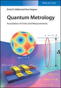
Pictures courtesy of A. Nicolaus (upper left hand corner, compare figure 7.4) and A. Müller (lower left hand corner, compare figure 6.10), Physikalisch-Technische Bundesanstalt, Braunschweig, Germany. Other picture courtesy of the authors.
All books published by Wiley-VCH are carefully produced. Nevertheless, authors, editors, and publisher do not warrant the information contained in these books, including this book, to be free of errors. Readers are advised to keep in mind that statements, data, illustrations, procedural details or other items may inadvertently be inaccurate.
Library of Congress Card No.: applied for
British Library Cataloguing-in-Publication Data
A catalogue record for this book is available from the British Library.
Bibliographic information published by the Deutsche Nationalbibliothek
The Deutsche Nationalbibliothek lists this publication in the Deutsche Nationalbibliografie detailed bibliographic data are available on the Internet at <http://dnb.d-nb.de>.
© 2015 Wiley-VCH Verlag GmbH & Co. KGaA, Boschstr. 12, 69469 Weinheim, Germany
All rights reserved (including those of translation into other languages). No part of this book may be reproduced in any form – by photoprinting, microfilm, or any other means – nor transmitted or translated into a machine language without written permission from the publishers. Registered names, trademarks, etc. used in this book, even when not specifically marked as such, are not to be considered unprotected by law.
Print ISBN: 978-3-527-41265-5
ePDF ISBN: 978-3-527-68089-4
ePub ISBN: 978-3-527-68092-4
Mobi ISBN: 978-3-527-68091-7
oBook ISBN: 978-3-527-68088-7
Cover Design Adam Design, Weinheim, Germany
Foreword
Measurements with ever-increasing precision and reliability are the fundamental basis of science and indispensable for progress in science, economy, and society. To ensure worldwide comparability of measurements, the Meter Convention was signed by 17 states in 1875 and its organs, the General Conference on Weights and Measures (Conférence Générale des Poids et Mesures, CGPM), the International Committee for Weights and Measures (Comité International des Poids et Mesures, CIPM), and the International Bureau of Weights and Measures (Bureau International des Poids et Mesures, BIPM), were established.
As of today, the Meter Convention counts 96 member states or associated states, includes 95 National Metrology Institutes and 150 Designated Institutes along with four international organizations, and, thus, represents not less than 97.6% of the total world economic power. Therefore, the International System of Units (Système International d'Unités), the SI, put in place by the 11th CGPM in 1960 as the basis for any measurement of any relevant quantity, provides a worldwide harmonized measurement and quality infrastructure enabling and fostering international trade around the globe.
The SI and its defined units, however, are not static but evolve as measurements are becoming more and more demanding and as science and technology proceeds. The remarkable progress in science, in particular in the area of laser physics, quantum optics, solid-state physics, and nanotechnology, has now paved the way for an upcoming fundamental revision of the SI. In the future, all SI units will be based on seven “defining constants,” among them are fundamental constants of nature like Planck's constant, the speed of light, or the charge of the electron, and, thus, will be independent of space and time with a relative accuracy below 10−16 according to state-of-the-art experiments.
The present book explains and illustrates the physics and technology behind these new SI definitions and their realization as well as their impact on measurements based on quantum physics phenomena. The book thus is essential, timely, and indeed urgently needed to communicate the envisaged revision of the SI and its consequences to the broad scientific community and other interested readership, including lecturers and teachers.
The authors are well qualified for this undertaking. Both have a long experience in metrology: Ernst Göbel has been the president of the PTB, the National Metrology Institute of Germany, for more than 16 years. He had been a member of the CIPM for more than 15 years and its president from 2004 to 2010. Uwe Siegner joined the PTB in 1999, working on metrological applications of femtosecond laser technology and on electrical quantum metrology. He is the head of the electricity division of the PTB since 2009. Both authors are experienced university lecturers, and in fact, the book is based on lectures given at the Technical University of Braunschweig.
I have studied the book with great interest and pleasure, and I wish the same to a broad readership.
Braunschweig,
November 2014
Prof. Dr. Joachim Ullrich,President of PTB,Vice President of CIPM,President of the Consultative Committee for Units (CCU)
Preface
The concept of some indivisible discrete single particles that are the basic building blocks of all matter goes back to philosophers many centuries BC. In particular, the Greek philosopher Demokrit and his students specified the idea of atoms (from the Greek àtomos) as the base elements of all matter.
These concepts found support in natural science beginning in the eighteenth century. This was particularly driven by chemistry (e.g., A. Lavoisier, J. Dalton, and D. Mendeleev), kinetic gas theory (e.g., J. Loschmidt and A. Avogadro), and statistical physics (e.g., J. Stefan, L. Boltzmann, and A. Einstein).
The discovery of the electron by J.J. Thomson (1897) and the results of the scattering experiments by J. Rutherford and his coworkers (1909) opened a new era in physics, based on their conclusions that atoms are not indivisible but instead composite species. In the atomic model developed by N. Bohr in 1913, the atom consists of electrons carrying a negative elementary charge (−e) and a tiny nucleus which carries almost all the mass of an atom composed of positively charged (+e) protons and electrically neutral neutrons. In Bohr's model, the electrons in an atom can only occupy discrete energy levels, consistent with the experimental findings of atom spectroscopy.
In the standard model of modern particle physics, electrons are in fact elementary particles belonging to the group of leptons. Protons and neutrons are composite particles composed of fractionally charged elementary particles, named quarks, which are bound together by the strong force.
In the last 50 years or so, scientists have learned to handle single quantum objects, for example, atoms, ions, electrons, and Cooper pairs, not least due to the tremendous progress in laser physics and nanotechnology. This progress has also laid the base for what we call “quantum metrology.” The paradigm of quantum metrology is to base measurements on the counting of discrete quanta (e.g., charge or magnetic flux quanta). In contrast, in classical metrology, the values of continuous variables are determined. Proceeding from classical to quantum metrology, the measurement of real numbers is replaced by counting of integers.
The progress in quantum metrology has also stimulated the discussion about a revision of the present International System of Units (Système International d'Unités), the SI. In particular, quantum metrology allows for a new definition of the base units of the SI in terms of constants of nature. This envisaged new definition of the SI as well as future possible revisions have actually set the frame of the present book.
The discrete nature of a physical system is sometimes obvious, for example, when considering microwave or optical transitions between discrete energy states in atoms or ions. The discrete quantum character of solid-state systems is less obvious because their single-particle energy spectra are quasicontinuous energy bands. Discrete quantum entities can then result from collective effects called macroscopic quantum effects.
The paradigm of quantum metrology becomes particularly obvious when the proposed new definition of the electrical units (ampere, volt, and ohm) is considered. We therefore give a more comprehensive description of the underlying solid-state physics and the relevant macroscopic quantum effects. For example, we partly summarize the textbook knowledge and deduce results starting from general principles in Chapter 4 where we introduce superconductivity, the Josephson effect, and quantum interference phenomena in superconductors.
This book addresses advanced students, research workers, scientists, practitioners, and professionals in the field of modern metrology as well as a general readership interested in the foundations of the forthcoming new SI definition. However, we consider this book as an overview which shall not cover all subjects in the same detail as it covers the electrical units. For further reading, we shall refer to the respective literature.
This book would not have been possible without the support of many colleagues and friends. We would like to especially mention Stephen Cundiff (JILA, now University of Michigan) and Wolfgang Elsäßer (University of Darmstadt) as well as our PTB colleagues Franz Ahlers, Peter Becker, Ralf Behr, Joachim Fischer, Frank Hohls, Oliver Kieler, Johannes Kohlmann, Stefan Kück, Ekkehard Peik, Klaus Pierz, Hansjörg Scherer, Piet Schmidt, Sibylle Sievers, Lutz Trahms, and Robert Wynands. We are also grateful for the technical support provided by Alberto Parra del Riego and Jens Simon. We further acknowledge the support of the present and former Wiley-VCH staff members, in particular Valerie Moliere, Anja Tschörtner, Heike Nöthe, and Andreas Sendtko.
Braunschweig,
April 2015
Ernst Göbel and Uwe Siegner
List of Abbreviations
2DEG
two-dimensional electron gas
AGT
acoustic gas thermometer/thermometry
AIST
National Institute of Advanced Industrial Science and Technology (National Metrology Institute of Japan)
APD
avalanche photo diode
BIPM
International Bureau for Weights and Measures (
Bureau International des Poids et Mesures
)
CBT
Coulomb blockade thermometer/thermometry
CCC
cryogenic current comparator
CCL
Consultative Committee for Length
CCM
Consultative Committee for Mass
CCT
Consultative Committee for Temperature
CCU
Consultative Committee for Units
CERN
European Organization for Nuclear Science
CGPM
General Conference on Weights and Measures (
Conférence Générale des Poids et Mesures
)
CIPM
International Committee for Weights and Measures (
Comité International des Poids et Mesures
)
CODATA
International Council for Science: Committee on Data for Science and Technology
CVGT
constant volume gas thermometer/thermometry
DBT
Doppler broadening thermometer/thermometry
DCGT
dielectric constant gas thermometer/thermometry
ECG
electrocardiography
EEG
electroencephalography
EEP
Einstein's equivalence principle
FQHE
fractional quantum Hall effect
GUM
Guide to the Expression of Uncertainty in Measurements
HEMT
high electron mobility transistor
IDMS
isotope dilution mass spectroscopy
INRIM
National Institute of Metrology of Italy (
Istituto Nazionale di Ricerca Metrologia
)
ISO
International Organization for Standards
ITS
International temperature scale
JNT
Johnson noise thermometer/thermometry
KRISS
Korea Research Institute of Standards and Science
LED
light-emitting diode
LNE
French Metrology Institute (
Laboratoire national de métrologie et d'essais
MBE
molecular beam epitaxy
MCG
magnetocardiography
MEG
magnetoencephalography
METAS
Federal Institute of Metrology, Switzerland
MOCVD
metalorganic chemical vapor deposition
MODFET
modulation-doped field-effect transistor
MOS
metal-oxide-semiconductor
MOSFET
metal-oxide-semiconductor field-effect transistor
MOT
magneto-optical trap
MOVPE
metalorganic vapor phase epitaxy
MSL
Measurement Standards Laboratory of New Zealand
NIM
National Institute of Metrology (National Metrology Institute of China)
NININ
normal metal/insulator/normal metal/insulator/normal metal
NIST
National Institute of Standards and Technology (National Metrology Institute of the United States)
NMR
nuclear magnetic resonance
NPL
National Physical Laboratory (National Metrology Institute of the United Kingdom)
NRC
National Research Council, Canada
PMT
photomultiplier tube
PTB
Physikalisch–Technische Bundesanstalt (National Metrology Institute of Germany)
QED
quantum electrodynamics
QHE
quantum Hall effect
QMT
quantum metrology triangle
QVNS
quantized voltage noise source
RCSJ
resistively–capacitively shunted junction
RHEED
reflection high-energy electron diffraction
RIGT
refractive index gas thermometer/thermometry
rms
root-mean-square
RT
radiation thermometry
SEM
scanning electron microscope/microscopy
SET
single-electron transport
SI
International System of Units (
Système International d'Unités
)
SINIS
superconductor/insulator/normal metal/insulator/superconductor
SIS
superconductor/insulator/superconductor
SNS
superconductor/normal metal/superconductor
SOI
silicon-on-insulator
SPAD
single-photon avalanche diode
SQUID
superconducting quantum interference device
TES
transition-edge sensor
TEM
transmission electron microscope/microscopy
TPW
triple point of water
UTC
coordinated universal time
XRCD
X-ray crystal density
YBCO
yttrium barium copper oxide
1Introduction
Metrology is the science of measurement including all theoretical and experimental aspects, in particular the experimental and theoretical investigation of the uncertainty of measurement results. According to Nobel Prize winner J. Hall, “metrology truly is the mother of science” [1].
Metrology, actually, is almost as old as mankind. As men began to exchange goods, they had to agree on commonly accepted standards as a base for their trade. And indeed, many of the ancient cultures like China, India, Egypt, Greece, and the Roman Empire had a highly developed measurement infrastructure. Examples are the Nippur cubit from the third millennium BCE found in the ruins of a temple in Mesopotamian and now exhibited in the archeology museum in Istanbul and the famous Egyptian royal cubit as the base length unit for the construction of the pyramids. Yet, the culture of metrology got lost during the Middle Ages when many different standards were in use. In Germany, for instance, at the end of the eighteenth century, 50 different standards for mass and more than 30 standards for length were used in different parts of the country. This of course had been a barrier to trade and favored abuse and fraud. It was then during the French revolution that the French Académie des Sciences took the initiative to define standards independent of the measures taken from the limbs of royal representatives. Instead, their intent was to base the standards on stable quantities of nature available for everyone at all times. Consequently, in 1799, the standard for length was defined as one 10 million part of the quadrant of the earth, and a platinum bar was fabricated to represent this standard (Mètre des Archives). Subsequently, the kilogram, the standard of mass, was defined as the mass of one cubic decimeter of pure water at the temperature of its highest density at 3.98 °C. This can be seen as the birth of the metric system which, however, at that time was not generally accepted through Europe or even in France. It was only with the signature of the Meter Convention in 1875 by 17 signatory countries that the metric system based on the meter and the kilogram found wider acceptance [2]. At the time of this writing, the Meter Convention has been signed by 55 states with another 41 states being associated with the General Conference on Weights and Measures (Conférence Générale des Poids et Mesures, CGPM). At the General Conferences, following the first one in 1889, the system of units was continuously extended. Finally, at the 11th CGPM in 1960, the present SI (Système International d'Unités) (see Section 2.2) with the kilogram, second, meter, ampere, kelvin, and candela as base units was defined. The mole, unit of amount of substance, was added at the 14th CGPM in 1971. Within the SI, the definition of some of the units has been adopted according to progress in science and technology; for example, the meter was defined in 1960 on the basis of the wavelength of a specific emission line of the noble gas krypton. But then, in 1983, it was replaced by the distance light travels in a given time and by assigning a fixed value to the speed of light in vacuum. Likewise, the second, originally defined as the ephemeris second, was changed by the 13th CGPM and defined via an electronic transition in the Cs isotope 133. Thus, today, the meter and the second are defined by constants of nature. At present, efforts to newly define the system of all units shall be based on constants of nature [3–7]. In fact, in this context, single quanta physics has a decisive role as will be outlined in this book.
We shall begin with introducing some basic principles of metrology in Chapter 2. We start in Section 2.1 by repeating some basic facts related to measurement and will discuss in particular the limitations for measurement uncertainty. The SI, in its present form, is summarized in Section 2.2 together with the proposed new definitions.
Chapter 3 is entitled laser cooling, atom clocks, and the second. Here, we describe the realization of the present definition of the second based on the hyperfine transition in the ground state of 133Cs employing laser-cooled atoms. We further describe recent developments of the so-called optical clocks, which have the potential for higher accuracy and stability than the present microwave clocks and will definitely lead to a revised definition of the second in the foreseeable future.
Chapter 4 is devoted to superconductivity and its utilization in metrology. Because of its prominent role for electrical metrology, we give an introduction to superconductivity, the Josephson effect, magnetic flux quantization, and quantum interference. By means of the Josephson effect, the volt (the unit for the electrical potential difference) is traced back to the Planck constant and the electron charge as realized in today's most precise voltage standards. Magnetic flux quantization and quantum interference allow the realization of quantum magnetometers (superconducting quantum interference devices) with unprecedented resolution and precision.
The underlying solid-state physics and the metrological application of the quantum Hall effect are discussed in Chapter 5. In Chapter 6, we describe the physics of single-electron transport devices and their potential for realizing the unit of electrical current, the ampere. The ampere is then traced back to the charge of the electron and frequency. Finally, the so-called metrological triangle experiment will be described.
Chapter 7 is then devoted to the envisaged new definition of the kilogram based on the Planck constant. In particular, we will present the watt balance and the silicon single crystal experiment for a precise determination of the Planck constant and the realization of the newly defined kilogram.
The envisaged new definition of the kelvin and various experiments to determine precisely the value of the Boltzmann constant are discussed in Chapter 8.
In Chapter 9, finally, we take an even further look into the future of the SI when we discuss the prospect of single-photon emitters for a possible new definition of radiometric and photometric quantities, for example, for (spectral) irradiance and luminous intensity.
References
1. Hall, J. (2011) Learning from the time and length redefinition, and the metre demotion.
Philos. Trans. R. Soc. A
,
369
, 4090–4108.
2. for a review on the development of modern metrology see e.g.: Quinn, T. and Kovalevsky, J. (2005) The development of modern metrology and its role today.
Philos. R. Soc. Trans. A
,
363
, 2307–2327.
3. Discussion Meeting issue “The new SI based on fundamental constants”, organized by Quinn, T. (2011)
Philos. Trans. R. Soc. A
,
369
, 3903–4142.
4. Mills, I.M., Mohr, P.J., Quinn, T.J., Taylor, B.N., and Williams, E.R. (2006) Redefinition of the kilogram, ampere, kelvin and mole: a proposed approach to implementing CIPM recommendation 1 (CI-2005).
Metrologia
,
43
, 227–246.
5. Flowers, J. and Petley, B. (2004) in
Astrophysics, Clocks and Fundamental Constants
(eds S.G. Karshenboim and E. Peik), Springer, Berlin, Heidelberg, pp. 75–93.
6. Okun, L.B. (2004) in
Astrophysics, Clocks and Fundamental Constants
(eds S.G. Karshenboim and E. Peik), Springer, Berlin, Heidelberg, pp. 57–74.
7. Leblond, J.-M. (1979) in
Problems in the Foundations of Physics; Proceedings of the International School of Physics “Enrico Fermi” Course LXXXII
(ed. G. Lévy Toraldo di Francia), North Holland, Amsterdam, p. 237.
2Some Basics
2.1 Measurement
Measurement is a physical process to determine the value (magnitude) of a quantity. The quantity value can be expressed as
where {q} is the numerical value and [Q] the unit (see following chapter). Repeated measurements of the same quantity, however, generally will result in slightly different results. In addition, systematic effects affecting the measurement result might be present and have to be considered. Thus, any measurement result must be completed by an uncertainty statement. This measurement uncertainty quantifies the dispersion of the quantity values being attributed to a measurand, based on the information used. Measurement uncertainty comprises, in general, many components. Some of these may be evaluated by type A evaluation of measurement uncertainty from the statistical distribution of the quantity values from series of measurements and can be characterized by standard deviations. The other components, which may be evaluated by type B evaluation of measurement uncertainty, can also be characterized by standard deviations, evaluated from probability density functions based on experience or other information. For the evaluation of uncertainties of measurements, an international agreed guide has been published jointly by ISO and the Bureau International des Poids et Mesures (BIPM), the Guide to the Expression of Uncertainty in Measurement (GUM) [1, 2]. Precision measurements generally are those with the smallest measurement uncertainty.
2.1.1 Limitations of Measurement Uncertainty
One might tend to believe that measurement uncertainty can be continuously decreased as more and more effort is put in the respective experiment. However, this is not the case since there are fundamental as well as practical limitations for measurement precision. The fundamental limit is a consequence of the Heisenberg uncertainty principle of quantum mechanics, and the major practical limit is due to noise.
2.1.1.1 The Fundamental Quantum Limit
Note that throughout this book, we will use the letter f to denote technical frequencies, while the Greek letter ν is used to denote optical frequencies.
The Heisenberg uncertainty principle is a fundamental consequence of quantum mechanics stating that there is a minimum value for the physical quantity action, H:
where h is the Planck constant. Action has the dimensions of energy multiplied by time and its unit is joule seconds. From the Heisenberg uncertainty principle, it follows that conjugated variables, like position and momentum or time and energy, cannot be measured with ultimate precision at a time. For example, if Δx and Δp are the standard deviation for position, x, and momentum, p, respectively, the inequality relation
holds (). Applied to measurement, the argument is as follows: in the course of a measurement, an exchange of information takes place between the measurement system and the system under consideration. Related to this is an energy exchange. For a given measurement time, τ, or bandwidth of the measurement system, , the energy which can be extracted from the system is limited according to Eq. (2.2) [3]:
Let us now consider, for example, the relation between inductance, L, and, respectively, magnetic flux, Φ, and current, I (see Figure 2.1). The energy is given by , and consequently,
Figure 2.1 Components and quantities considered (left) and the minimum current, Imin, and the minimum magnetic flux, Φmin, versus inductance, L, for an ideal coil.
(From [3], with kind permission from Wiley-VCH.)
These relations are depicted also in Figure 2.1. The gray area corresponds to the regime which is accessible by measurement. Please note that this is a heuristic approach which does not consider a specific experiment. Nevertheless, it may provide useful conclusions on how to optimize an experiment. For instance, if an ideal coil (without losses) shall be applied to measure a small current, the inductivity should be large (e.g., , , and then ). If instead the coil is applied to measure magnetic flux, L should be small (e.g., , , and then where is the ).
Likewise, for a capacitor with capacitance, C, the energy is given by
and thus,
Finally, for a resistor with resistance, R, the energy is given by
and thus, for the minimum current and voltage, respectively, we obtain
2.1.1.2 Noise
In this chapter, we briefly summarize some aspects of noise theory. For a more detailed treatment of this important and fundamental topic, the reader is referred to, for example, [4].
Noise limits the measurement precision in most practical cases. The noise power spectral density, P(T, f)/Δf, can be approximated by (Planck formula)
where f is the frequency, kB the Boltzmann constant, and T the temperature. Two limiting cases can be considered as follows.


