100,99 €
Mehr erfahren.
- Herausgeber: John Wiley & Sons
- Kategorie: Wissenschaft und neue Technologien
- Sprache: Englisch
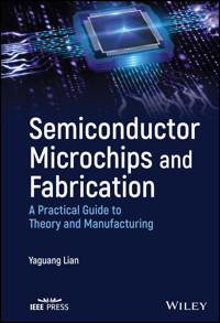
Semiconductor Microchips and Fabrication
Advanced and highly illustrated guide to semiconductor manufacturing from an experienced industry insider
Semiconductor Microchips and Fabrication is a practical yet advanced book on the theory, design, and manufacturing of semiconductor microchips that describes the process using the principles of physics and chemistry, fills in the knowledge gaps for professionals and students who need to know how manufacturing equipment works, and provides valuable suggestions and solutions to many problems that students or engineers often encounter in semiconductor processing, including useful experiment results to help in process work.
The explanation of the semiconductor manufacturing process, and the equipment needed, is carried out based on the machines that are used in clean rooms over the world so readers understand how they can use the equipment to achieve their design and manufacturing ambitions. Combining theory with practice, all descriptions are carried out around the actual equipment and processes by way of a highly visual text, with illustrations including equipment pictures, manufacturing process schematics, and structures of semiconductor microchips.
Sample topics covered in Semiconductor Microchips and Fabrication include:
- An introduction to basic concepts, such as impedance mismatch from plasma machines and theories, such as energy bands and Clausius-Clapeyron equation
- Basic knowledge used in semiconductor devices and manufacturing machines, including DC and AC circuits, electric fields, magnetic fields, resonant cavity, and the components used in the devices and machines
- Transistor and integrated circuits, including bipolar transistors, junction field effect transistors, and metal-semiconductor field effect transistors
- The main processes used in the manufacturing of microchips, including lithography, metallization, reactive-ion etching (RIE), plasma-enhanced chemical vapor deposition (PECVD), thermal oxidation and implantation, and more
- The skills in the design and problem solving of processes, such as how to design a dry etching recipe, and how to solve the micro-grass problems in Bosch process
Through Semiconductor Microchips and Fabrication, readers can obtain the fundamental knowledge and skills of semiconductor manufacturing, which will help them better understand and use semiconductor technology to improve their product quality or project research. Before approaching this text, readers should have basic knowledge of physics, chemistry, and circuitry.
Sie lesen das E-Book in den Legimi-Apps auf:
Seitenzahl: 445
Veröffentlichungsjahr: 2022
Ähnliche
IEEE Press
445 Hoes Lane Piscataway, NJ 08854
IEEE Press Editorial Board
Sarah Spurgeon,
Editor in Chief
Jón Atli Benediktsson
Andreas Molisch
Diomidis Spinellis
Anjan Bose
Saeid Nahavandi
Ahmet Murat Tekalp
Adam Drobot
Jeffrey Reed
Peter (Yong) Lian
Thomas Robertazzi
Semiconductor Microchips and Fabrication
A Practical Guide to Theory and Manufacturing
Yaguang Lian
University of Illinois
Urbana, USA
Copyright © 2023 by The Institute of Electrical and Electronics Engineers, Inc. All rights reserved.
Published by John Wiley & Sons, Inc., Hoboken, New Jersey.
Published simultaneously in Canada.
No part of this publication may be reproduced, stored in a retrieval system, or transmitted in any form or by any means, electronic, mechanical, photocopying, recording, scanning, or otherwise, except as permitted under Section 107 or 108 of the 1976 United States Copyright Act, without either the prior written permission of the Publisher, or authorization through payment of the appropriate per-copy fee to the Copyright Clearance Center, Inc., 222 Rosewood Drive, Danvers, MA 01923, (978) 750-8400, fax (978) 750-4470, or on the web at www.copyright.com. Requests to the Publisher for permission should be addressed to the Permissions Department, John Wiley & Sons, Inc., 111 River Street, Hoboken, NJ 07030, (201) 748-6011, fax (201) 748-6008, or online at http://www.wiley.com/go/permission.
Limit of Liability/Disclaimer of Warranty: While the publisher and author have used their best efforts in preparing this book, they make no representations or warranties with respect to the accuracy or completeness of the contents of this book and specifically disclaim any implied warranties of merchantability or fitness for a particular purpose. No warranty may be created or extended by sales representatives or written sales materials. The advice and strategies contained herein may not be suitable for your situation. You should consult with a professional where appropriate. Neither the publisher nor author shall be liable for any loss of profit or any other commercial damages, including but not limited to special, incidental, consequential, or other damages.
For general information on our other products and services or for technical support, please contact our Customer Care Department within the United States at (800) 762-2974, outside the United States at (317) 572-3993 or fax (317) 572-4002.
Wiley also publishes its books in a variety of electronic formats. Some content that appears in print may not be available in electronic formats. For more information about Wiley products, visit our web site at www.wiley.com.
Library of Congress Cataloging-in-Publication Data Applied for:
Hardback ISBN: 9781119867784
Cover Design: Wiley
Cover Image: © Den Rise/Shutterstock
Author Biography
Yaguang Lian is a research engineer in Holonyak Micro & Nanotechnology Lab at the University of Illinois at Urbana-Champaign (UIUC). In 1979, he studied at the Department of Electronics, Hebei University, China. In 1983, with a bachelor's degree, he worked on silicon epitaxy for a semiconductor company for two years. Yaguang returned to Hebei University as a graduate student in 1985. In 1988, he got his master's degree. From 1988 to 2001, he worked with Hebei Semiconductor Research Institute (HSRI). In 2001, Yaguang joined a start-up company at California as a senior semiconductor process engineer. Two years later, he worked in the University of California, Los Angeles (UCLA). From November 2004 till now, Yaguang works as research engineer at the University of Illinois.
With over 35 years of experience in the semiconductor field, Yaguang has dealt with different processes for different kinds of semiconductors, such as Si and GaAs. When he worked in HSRI in China, he was manufacturing GaAs MESFET digital IC and designing circuits, and also managed a process flow from implantation to packaging. In the company at California, he worked mainly in the manufacture of silicon optical waveguide. At UCLA, Yaguang started the equipment repair and maintenance, and users' training, which he further evolved at UIUC. He is also responsible for designing different recipes to meet the needs of professors in different projects, such as dry etching of silicon, III–V materials, dielectric films and metals, and deposition of silicon nitride film with different stresses. He solves different types of process problems for students paving way for their research.
Yaguang believes that to be a good engineer, one must have an important trait, which is “it is not enough for you to know how to do it, you must know why to do it.”
Preface
“Semiconductor process engineer” is the label of my whole career. As a research engineer, I have been working in Holonyak Micro & Nanotechnology Laboratory (HMNTL) at the University of Illinois for nearly two decades. The core part of HMNTL is the clean room with different types of equipment, which are used to fabricate various semiconductor devices. The lab is open to the campus and society. Up to now, I have trained thousands of users in using the lab machines. Most users are doctoral students. These training experiences have given me the opportunities to encounter various issues and solve different technical problems with different kinds of users.
During my years of training, I have met students with different backgrounds. Most of them have EE or ECE backgrounds, and some of them don't have these backgrounds. The student without EE or ECE backgrounds lack basic knowledge of semiconductors and processing, while students majoring in EE or ECE need to make up the working principles of manufacturing processes and the basic structures of equipment. Lack of adequate understanding of process and equipment not only occurs in many doctoral students with backgrounds in EE or ECE, but also in some postdoctoral researchers. An important reason for this phenomenon is that they do not understand the process and equipment from the perspective of physical and chemical principles. These issues and the encouragement from students drove me to write this book.
We are using microchips to describe semiconductor devices and integrated circuits (ICs). To meet the needs of readers without EE or ECE backgrounds, this book includes the knowledge of semiconductor concepts, theories, histories, and basic structures of microchips, which help to lay the foundation for them to understand semiconductor manufacturing processes. To help the readers with EE or ECE backgrounds better understand the process and equipment, this book strives to clarify the principles of processes, the basic structures of equipment, and the design of process recipes based on the physical laws, chemical reactions, and electrical circuit theories. It not only shows readers how to do the process, but also explains why the process is designed in such a way. It combines the processes with the actual machines used in the clean room at the University. Therefore, the book will be very useful for readers with different backgrounds.
This is a handy book for many audiences as it starts with the basic concepts and daily examples. It uses simple language to explain complicated concepts and theories. The needs of various levels of audiences will be satisfied, such as undergraduates, graduates, researchers, engineers, and professors. The book will pave the ways for readers in their semiconductor research, process, and manufacture. From this book, readers can find many valuable suggestions and solutions to the problems that students or engineers often encounter in semiconductor processing. These suggestions and solutions are based on my years of working experience. Moreover, readers can also find some useful experimental results in the book, which will help them in their processing work.
Nowadays, semiconductors are widely used in many fields. This book is also written for those who are not majoring but interested in the research and production of semiconductor microchips. Even those who do not have enough knowledge of semiconductor and processes, as long as they have basic knowledge of physics, chemistry, and circuit, after reading this book, can easily learn and quickly grasp the principles, knowledge, and manufacturing processes of semiconductors. From this book, readers can obtain the fundamental concepts and skills, which will be a necessity in the development of semiconductor processing. They can apply all these concepts and skills in semiconductor technology to improve their product quality or the project research.
I could not accomplish my book without HMNTL. In HMNTL, I have gotten a good time with my colleagues. I would like to express my appreciation to my excellent colleagues: Mr. John Hughes, Dr. Mark McCollum, Dr. Edmond Chow, Dr. Glennys Mensing, Ken Tarman, Hal Romans, Michael Hansen, Lavendra Mandyam, Karthick Jeganathan, Paul DiPippo. From them, I have learned more about the layout and management of the clean room at the university. From them, I also have gotten a lot of help in the equipment troubleshooting, recipe design, and parameter testing. I am so glad that I have worked with them for so many years.
In writing this book, many friends have offered their support. Dr. Ruijie Zhao gave me good advice at the beginning. Dr. Wenjuan Zhu reviewed the draft. Dr. Anming Gao pushed me to write the book. Mr. Raman Kumar and Alvin Flores provided me good suggestions on some theoretical issues, and some students supplied me with nice images. I especially thank Tianyi Bai, my nephew, a graduate student at the University of Pennsylvania, who has given me valuable opinions in some areas. Finally, I would like to thank the Internet, which was born from semiconductor technology. From the Internet, I can easily find the information I need. Here, I deeply appreciate the companies and individuals who agreed to let me use their images in the book.
February 12, 2022 Yaguang Lian
University of Illinois at Urbana-Champaign
Champaign, IL
1Introduction to the Basic Concepts
1.1 What Is a Microchip?
Looking back on the development history of human society, it has gone through different stages of civilization, from the primitive stone age to the modern information age. The material used to support stone age was stone. The material used to support information age is semiconductor. So contemporary society is essentially a semiconductor era represented by silicon. This era began in the late 1950s and early 1960s in the Bay Area of Northern California near San Francisco in the United States. Later, people called this area “Silicon Valley,” the sign of high technology (abbreviated to high-tech), which have brought us into the information age. Silicon and other semiconductors are the cornerstone of this era. If petroleum is thought as the blood of modern society, semiconductor microchips can be regarded as the brain. Semiconductor technology has been integrated by different industries to enhance their technical level, and it has also come into our households. A microchip is a semiconductor device or an integrated circuit (IC). An IC is to make a lot of tiny semiconductor devices onto a small flat piece of semiconductor (a die).
1.2 Ohm's Law and Resistivity
Due to microchips are operated by electricity, so first, let us get to know what electricity is, and how electricity works. See Figure 1.1. It is a voltage converter for a small household electronic product. The explanation of some technical words on the converter are listed as follows:
“VAC” means “Volts Alternating Current”
“Hz-Hertz” is the frequency unit
“W-Watt” is the unit of power
“mA” means “milli-Ampere.” “Ampere-A” is the unit of electric current (abbreviated to current)
Figure 1.1 A voltage converter for an electronic product.
Source: Harman International Industries, Incorporated.
Among them, voltage, current, and watt are the three basic parameters used to express the characteristics of electricity. Another basic parameter is resistance, we will talk about it in Ohm's law below.
Electricity is the set of physical phenomena. A physical phenomenon refers to a process that does not produce new substances, such as the movement of objects, the freezing and boiling of water, and so on. Corresponding to this is a chemical phenomenon, which refers to a process that can produce new substances. We call this process a chemical reaction, for example, oxygen and hydrogen generate water through a chemical reaction. There is also a nuclear phenomenon, which is beyond the scope of this book and will not be discussed. Now, let us return to the topic of electricity. Electricity is generated by the motion of matter that has a property of electric charge. An electric charge can be positive or negative. Positive one is called “positive charge” and represented by “+.” Negative one is called “negative charge” and represented by “−.” The movement of electric charges is an electric current. In most cases, the current is produced by the movement of electrons, which are negative charges. The unit of electric current, Ampere, is named in honor of a French mathematician and physicist André-Marie Ampère (1775–1836), who is considered the father of electrodynamics.
Electricity comes into our homes through electrical wires and then goes to various electrical appliances. There are usually two kinds of electrical wires (abbreviated to wire) for household use. They are two-core wires, just like the wire attached to the converter in Figure 1.1, and three-core wires. If we strip a three-core wire, its structure is shown in Figure 1.2. “Cable Jacket” is the insulating sheath, “Wire Insulation” is the insulating layer, and “Stripped Wire” is the wire exposed after the insulating layer is stripped. The three wires are hot, neutral, and ground. Most of the insulating sheathes and layers are made of rubber and plastic; the wire is made of metal. In most cases, the metal is aluminum or copper. The kind of materials such as rubber and plastic are called insulators, in which, electrons cannot move. Thus, current cannot flow in the insulators. We call aluminum and copper, the type of materials, conductors, because electrons can move in them. Thus, electrical current can flow in the conductors.
Figure 1.2 The basic structure of three-core wire.
All materials are composed of atoms, and atoms will hinder the movement of electrons, which means that all materials have resistance in the opposite direction of the current flow. This resistance is called electrical resistance (abbreviated to resistance), and the unit of the resistance is Ohm, which is represented by “Ω.” Ω is named in honor of the German physicist Georg Simon Ohm (March 16, 1789–July 6, 1854). How do electrons move in a conductor to generate the current? They are driven by the pressure of electricity. This special pressure is called voltage, and the unit is volt, which is expressed by “V.” The voltage unit volt is to commemorate the Italian physicist Alessandro Volta (1745–1827), who invented voltaic pile, the first electrical battery in the world. Now, we have three parameters related to electricity: current, represented by “I”; resistance, represented by “R”; voltage, represented by “V.” Sometimes lowercase letters are also used to indicate current, resistance, and voltage. The relationship between them is the famous Ohm's law:
Why can electrons flow in metal? It is because the metal has little resistance; electrons cannot flow in the insulator because the insulator has large resistance. Scientists use resistivity to express the resistance of a material per unit length. “ρ” is used to represent resistivity, its unit is ohm · cm (Ω · cm). The relationship between resistance and resistivity is expressed by the following formula:
Figure 1.3 A diagram of a section of resistive material, current flows along the length direction.
Source: Reproduced with permission of Physics LibreTexts.
See Figure 1.3, where “A” is the cross-sectional area, and “L” is the length of a piece of material. To make more convenient for practical use, we introduce the concept of conductance. The symbol of conductance is G, and the relationship with resistance R is as follows:
The unit of G is Siemens and is represented by the letter S to commemorate Werner von Siemens (December 13, 1816–December 6, 1892). He was a German scientist and founder of Siemens. Correspondingly, there is conductivity, expressed by σ, and the relationship with resistivity ρ is
In practical application, we often use devices called resistors, which are shown in the left of Figure 1.4, and the symbol is shown in the right of Figure 1.4.
Figure 1.4 The picture of resistors (a) and the symbol (b).
Source: Reproduced with permission of SparkFun Electronics.
1.3 Conductor, Insulator, and Semiconductor
Now, we use resistivity to distinguish conductors and insulators. In general, the resistivity of a conductor is very low, and the resistivity of an insulator is very high. For example, the resistivity of copper is 1.55 × 10⁻⁶ Ω · cm, and for aluminum is 2.5 × 10⁻⁶ Ω · cm [1], where 10−6 is one millionth. Polyvinyl chloride (PVC) is a kind of plastic commonly used for making insulating materials, its resistivity is 2 × 10¹²–2 × 10¹⁴ Ω · cm, nylon is 4.56 × 10¹⁶ Ω · cm [2]. Mathematically, 102 means there is a zero after 10, 103 means there are two zeros after 10, and so on. From which, we can know that the resistivity of the above two insulating materials has 11–15 zeros after 10. Conductors and insulators have the resistivities either extremely small or extremely large. Does a material with resistivity between them exist? Yes, this material exists, we call it a semiconductor. At room temperature, the resistivity of silicon is 6.3 × 10⁴ Ω · cm, and the resistivity of germanium is 46 Ω · cm [1]. Silicon with the symbol Si is the most important material in the modern semiconductor industry. That is why the Bay Area of Northern California is called Silicon Valley. Germanium with the symbol Ge was used to make the first transistor in the world. Silicon and germanium are single-element semiconductors. Another kind of semiconductors are compound semiconductors. The most used one is gallium arsenide with symbol GaAs, which has a resistivity of 107–109 Ω · cm [3]. With such a high resistivity, we call this material a semi-insulator. Due to the high resistivity, pure GaAs cannot be used to make a device. It must be changed to a semiconductor by a process of doping. In fact, silicon also needs to be doped to make devices. We will discuss doping process in Chapter 17.
So far, by using the resistivity, we have distinguished between conductors, semiconductors, semi-insulators, and insulators. Generally, semi-insulating materials represented by GaAs need to be converted into semiconductors before they can be used to make devices. So, in the following discussion, we will classify semi-insulating materials as semiconductors. It is too simple to distinguish materials from resistivity. To really understand them, especially semiconductors, we have to use quantum mechanics and energy band theory. It is necessary for us to give a brief introduction of quantum mechanics and energy band theory.
References
1
饭田修一等, (1979). 物理学常用数表, [日]. 科学出版社, 133–135.
2
Fink, D.G. and Beaty, H.W. (1987).
Standard Handbook for Electrical Engineers
, 12e, 4–153. McGraw-Hill Companies.
3
Soares, R., Graffeuil, J., and Obrégon, J. (1983).
Applications of GaAs MESFETs
, 17. Artech House.
2Brief Introduction of Theories
This chapter is a brief introduction of quantum mechanics, and then energy band theory. By using these theories, we can easily understand what is a conductor, an insulator, and a semiconductor.
2.1 The Birth of Quantum Mechanics
At the end of the nineteenth century and the beginning of the twentieth century, Newtonian mechanics, Maxwell's theory of the electromagnetic field, and Maxwell–Boltzmann statistics constituted what is now called classical physics that ruled the physical world at that time. The physical quantities discussed in classical physics have two characteristics: continuity and controllability. However, there were two problems that could not be solved by using the theory of classical physics. One was blackbody radiation, and the other was Michelson–Morley experiment. In 1900, Max Planck (April 23, 1858–October 4, 1947), a German theoretical physicist proposed that in the radiation and absorption of electromagnetic field, the energy appeared in a discrete rather than continuous form. This discrete energy is called the quantization of energy. This assumption explains blackbody radiation very well and is considered as the beginning of quantum mechanics. In 1905, Albert Einstein (March 14, 1879–April 18, 1955) published the theory of special relativity to explain Michelson–Morley experiment. Since then, physics has entered the post-Newtonian era of modern physics.
According to Planck's assumption, each part of energy is proportional to the frequency of electromagnetic radiation. We use E to represent the energy and ν to represent the frequency. The Plank's equation is
The “h” here is called Planck's constant. The frequency is the number of occurrences of a repeating event per unit of time. In most cases, frequency is represented by the letter “ƒ.” However, in quantum mechanics it is represented by “ν.” “T” is used to represent the period. It is the duration of time of one cycle in a repeating event. The relationship between ƒ and T is as follows:
If we use seconds to express time, then unit of frequency is Hertz (Hz), named after German physicist Heinrich Hertz (February 22, 1857–January 1, 1894). He used the experiment to confirm the existence of electromagnetic waves. Electromagnetic waves were theoretically predicted by James Clerk Maxwell (June 13, 1831–November 5, 1879). The theory is well-known as Maxwell's equations. The experiment also proved that the light is electromagnetic waves that were predicted by Maxwell.
Planck's Eq. (2.1) plays a very important role in physics. It is one of key differences between classic physics and modern physics. In classic physics, the energy is supposed to exist in the continuous form and is valid at a large (macroscopic) scale. The Planck equation points out that at small (microscopic) scale, energy exists in the discrete (quantum) form, which is one of the basic characteristics of quantum mechanics. Therefore, when dealing with microscopic worlds such as atoms and subatomic particles, we must use quantum mechanics.
In 1905, Einstein published four papers – photoelectric effect, Brownian motion, special theory of relativity, and mass–energy equivalence. These four articles contributed substantially to the foundation of modern physics and changed people's views from beginning of history on space, time, mass, and energy. So this year is also called the “miracle year” of physics. In the paper of mass–energy equivalence, Einstein wrote down a well-known equation:
In this equation, E is energy, m is mass, c is the speed of light, c = 300 000 km/s.
Now, let us talk about photoelectric effect. The effect means that when light beams shine on the surface of an object (mostly metal), and if the light frequency is higher than a certain number, the electrons on the surface will be excited and escape from the object. This phenomenon was first discovered by Hertz. The escaped electrons are called photoelectrons. In the paper of photoelectric effect, Einstein assumed that light travel through space, not in the form of waves as described in the classical theory of electromagnetic field, but in discrete “wave packets.” A wave packet is called a “photon.” A photon obeys Planck's equation and has energy of hν. When the frequency (energy) of photons that are illuminating the object reaches or exceeds a certain threshold frequency, electrons will be emitted out of the surface of the object (see Figure 2.1).
In 1913, Niels Bohr (October 7, 1885–November 18, 1962), a Danish physicist, and Ernest Rutherford (August 30, 1871–October 19, 1937), a British physicist born in New Zealand, together proposed a model to describe atoms. This model states that an atom contains small, high-density nucleus, surrounded by electrons. This is like the structure of the solar system, except that this attraction comes from electromagnetic force rather than gravity. We call this model Rutherford–Bohr model, or simply Bohr model. Figure 2.2 is Bohr model of a hydrogen atom. In this figure, the nucleus is in the center, which is composed of a neutron and a proton. An electron rotates in outer orbits. Neutron is uncharged and proton is positively charged. Since the number of protons in an atom is the same as the number of electrons, under normal circumstances, the at
