140,99 €
Mehr erfahren.
- Herausgeber: John Wiley & Sons
- Kategorie: Wissenschaft und neue Technologien
- Sprache: Englisch
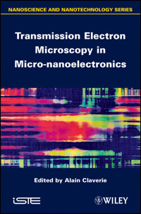
Today, the availability of bright and highly coherent electron sources and sensitive detectors has radically changed the type and quality of the information which can be obtained by transmission electron microscopy (TEM). TEMs are now present in large numbers not only in academia, but also in industrial research centers and fabs. This book presents in a simple and practical way the new quantitative techniques based on TEM which have recently been invented or developed to address most of the main challenging issues scientists and process engineers have to face to develop or optimize semiconductor layers and devices. Several of these techniques are based on electron holography; others take advantage of the possibility of focusing intense beams within nanoprobes. Strain measurements and mappings, dopant activation and segregation, interfacial reactions at the nanoscale, defect identification and specimen preparation by FIB are among the topics presented in this book. After a brief presentation of the underlying theory, each technique is illustrated through examples from the lab or fab.
Sie lesen das E-Book in den Legimi-Apps auf:
Seitenzahl: 406
Veröffentlichungsjahr: 2013
Ähnliche
Contents
Introduction
Chapter 1 Active Dopant Profiling in the TEM by Off-Axis Electron Holography
1.1. Introduction
1.2. The Basics: from electron waves to phase images
1.3. Experimental electron holography
1.4. Conclusion
1.5. Bibliography
Chapter 2 Dopant Distribution Quantitative Analysis Using STEM-EELS/EDX Spectroscopy Techniques
2.1. Introduction
2.2. STEM-EELS-EDX experimental challenges for quantitative dopant distribution analysis
2.3. Experimental conditions for STEM spectroscopy impurity detection
2.4. STEM EELS-EDX quantification of dopant distribution application examples
2.5. Discussion on the characteristics of STEM-EELS/EDX and data processing
2.6. Bibliography
Chapter 3 Quantitative Strain Measurement in Advanced Devices: A Comparison Between Convergent Beam Electron Diffraction and Nanobeam Diffraction
3.1. Introduction
3.2. Electron diffraction technique in TEM (CBED and NBD)
3.3. Experimental details
3.4. Results and discussion
3.5 Conclusion
3.6. Bibliography
Chapter 4 Dark-Field Electron Holography for Strain Mapping
4.1. Introduction
4.2. Setup for dark-field electron holography
4.3. Experimental requirements
4.4. Strained silicon transistors with recessed sources and drains stressors
4.5. Thin film effect
4.6. Silicon implanted with hydrogen
4.7. Strained silicon n-MOSFET
4.8. Understanding strain engineering
4.9. Strained silicon devices relying on stressor layers
4.10. 28-nm technology node MOSFETs
4.11. FinFET device
4.12. Conclusions
4.13 Bibliography
Chapter 5 Magnetic Mapping Using Electron Holography
5.1. Introduction
5.2. Experimental
5.3. Hologram analysis: from the phase images to the magnetic properties
5.4. Resolutions
5.5. One example: FePd (L10) epitaxial thin film exhibiting a perpendicular magnetic anisotropy (PMA)
5.6. Prospective and new developments
5.7. Conclusions
5.8. Bibliography
Chapter 6 Interdiffusion and Chemical Reaction at Interfaces by TEM/EELS
6.1. Introduction
6.2. Importance of interfaces in MOSFETs
6.3. TEM and EELS
6.4. TEM/EELS and study of interdiffusion/chemical reaction at interfaces in microelectronics
6.5. HRTEM/EELS as a support to developments of RE- and TM-based HK thin films on Si and Ge
6.6. Conclusion
6.7. Bibliography
Chapter 7 Characterization of Process-Induced Defects
7.1. Interfacial dislocations
7.2. Ion implantation induced defects
7.3. Conclusions
7.4. Bibliography
Chapter 8 In Situ Characterization Methods in Transmission Electron Microscopy
8.1. Introduction
8.2. In situ in a TEM
8.3. Biasing in a conventional TEM
8.4. Sample design
8.5. Conclusions
8.6. Bibliography
Chapter 9 Specimen Preparation for Semiconductor Analysis
9.1. The focused ion beam tool
9.2. Ion-sample interaction
9.3. Beam currents and energies for specimen preparation
9.4. Practical specimen preparation
9.5. In situ lift-out
9.6. H-bar technique
9.7. Broad beam ion milling
9.8. Mechanical wedge polishing
9.9. Conclusion
9.10. Bibliography
List of Authors
Index
First published 2013 in Great Britain and the United States by ISTE Ltd and John Wiley & Sons, Inc.
Apart from any fair dealing for the purposes of research or private study, or criticism or review, as permitted under the Copyright, Designs and Patents Act 1988, this publication may only be reproduced, stored or transmitted, in any form or by any means, with the prior permission in writing of the publishers, or in the case of reprographic reproduction in accordance with the terms and licenses issued by the CLA. Enquiries concerning reproduction outside these terms should be sent to the publishers at the undermentioned address:
ISTE Ltd
27-37 St George’s Road
London SW19 4EU
UK
www.iste.co.uk
John Wiley & Sons, Inc.
111 River Street
Hoboken, NJ 07030
USA
www.wiley.com
© ISTE Ltd 2013
The rights of Alain Claverie to be identified as the author of this work have been asserted by him in accordance with the Copyright, Designs and Patents Act 1988.
Library of Congress Control Number: 2012952185
British Library Cataloguing-in-Publication Data
A CIP record for this book is available from the British Library
ISBN: 978-1-84821-367-8
Introduction
The MOS (Metal Oxyde Semiconductor) transistor is the key component driving the electronic logic revolution for the past 50 years ever since what has become known as Moore’s law was first published [MOR 65]. Moore claimed that the number of components inside a single chip would rise exponentially, increasing by a factor of two every year and a half. After 50 years and 30 technology nodes, and despite the fact that some physicists had predicted a real MOS limit for 50 nm gate lengths and below, Moore’s law still does not show any inflexion. The transistor gate length has continued to decrease from a few microns to a few tens of nanometers and the number of components per chip has crossed over the billions. This trend continues at a constant speed, respecting the initial Moore’s law. Why then are the limitations predicted in the literature still not observed? First, these limitations were based on the idea that evolution was only a matter of scaling and that ultimate transistors would look like the old transistors, that is planar, mostly made up of conventional Si and SiO2 and fabricated using basically the same processes of that in the 1980s. In fact, transistors still evolve because new materials are being integrated; they are built following new architectural rules and fabricated using different, alternative, processes.
Although the “scaling down” evolution was accompanied, and sometimes even guided, by process simulations that were based on robust, well-understood and physics-based modeling, today’s evolution is more complex, sometimes looking erratic, and involves exotic materials of uncertain physical and chemical characteristics, packed together using processes in which thermodynamics plays at best a second role. More than ever before, it is necessary to experimentally access the exact chemical composition and the crystalline state of these components with an extraordinary sensitivity and at nanometer resolution. This is the prerequisite condition, which is used not only to validate technological options, but most importantly to invent and calibrate the new generation of process simulators that will again be needed to continue the incredible adventure of microelectronics.
At the same time, transmission electron microscopy (TEM) is experiencing a revolution. For many years, TEM, seen by some as the last avatar of the optical microscope, had pursued the dream of “seeing the atoms”, concentrating mostly on improving the spatial resolution. Well, this is done, and no one doubts that high-resolution TEM did help considerably in figuring out how materials are made. However, today’s availability of highly coherent electron sources, sensitive detectors, imaging filters and particularly aberration correctors has radically changed the type and quality of the information that can be obtained by TEM.
The first revolution comes from the “possibility to image fields” using electron holography. The possibility of quantifying, and mapping, electrostatic fields within a device is a smart answer to the everlasting question of “where are the active dopant atoms?” Mapping the strain fields introduced in the channel of a device to boost carrier mobility is mandatory to understand and optimize its performance. Moreover, the combination of intense nanoprobes and sensitive detectors can be used to dose impurity contents and identify chemical compounds that may form, intentionally or not, in the course of processing.
This book aims to present in a simple and practical way the new quantitative techniques based on TEM that have been recently invented or developed to address most of the challenging issues scientists and process engineers face to characterize or optimize semiconductor layers and devices. Several of these techniques are based on electron holography; others take advantage of the possibility to focus on intense beams within nanoprobes. Strain measurements and mappings, dopant activation and segregation, interfacial reactions at the nanoscale, defects identification, in situ experiments and specimen preparation by Focused Ion Beam (FIB) are among the topics presented in this book. After a brief presentation of the underlying theory, each technique is illustrated through examples from the lab or from the fab.
TEMs are now present in large numbers not only in academic but also in industrial research centers and fabrication plants. Some of the techniques introduced above and extensively described in the following chapters are not widespread, sometimes suffering from the a priori statement that they are “difficult”. We believe that it is not the case and hope to convince every reader, scientist or engineer to set up and use these techniques in his or her own environment taking advantage of the “existing” or “to be bought soon” equipment.
The authors of this book have lots of experience in characterizing “real” devices, answering materials science questions arising when trying to accompany, sometimes guide, technological developments aimed at rendering electronic devices smaller, faster and cheaper while consuming less energy. This experience has been gained through daily work in public (CNRS and CEA) or private (STMicroelectronics) laboratories, often collaborating together within projects or networks financially supported by several institutions among which we want to cite the European Commission (FP6 then FP7 programs), the French ANR (White and R2N programs) and MINEFI (Alliance Nano2012) and the CNRS (METSA Network). We sincerely thank all of them for their support and help in developing and installing TEM as the indispensable companion tool of research and industry along the nanoelectronics pathway.
Bibliography
[MOR 65] MOORE G. E., “Cramming more components onto integrated circuits”, Electronics, vol. 38, no. 8, pp. 114–117, April 1965.
Chapter 1
Active Dopant Profiling in the TEM by Off-Axis Electron Holography
1.1. Introduction
Electron holography is a powerful transmission electron microscopy (TEM)-based technique that can be used to measure the phase change of an electron wave that has passed through a region of interest compared to the phase of an electron wave that has passed through only a vacuum. As the phase of an electron is sensitive to the magnetic, electrostatic and strain fields that can be found in and around a specimen, electron holography is a unique method that can be used to recover all of these properties with nanometer-scale resolution. The electrostatic potential in semiconductor materials is modified by the presence of active dopants. At this time, when only a few dopant atoms can affect the properties of an electronic device, electron holography provides a unique opportunity to look inside these devices and to learn about the activity of the dopant atoms. Characterization techniques such as secondary ion mass spectrometry and atom probe tomography cannot differentiate between active and inactive dopants. Other techniques such as scanning capacitance microscopy and scanning spreading resistance microscopy, which are capable of measuring the active dopants at the surface of specimens, may well have problems adapting to the latest generations of semiconductor materials that can consist of doped nanowires and three-dimensional structures. Therefore, electron holography is unique in that it allows the position of active dopants to be measured inside a specimen with 1 nm spatial resolution today [COO 11], and potentially atomic resolution in the future.
It was Gabor who introduced electron holography in his paper “Microscopy by Reconstructed Wavefronts” in 1948 [GAB 48]. Gabor realized that the measurement of the phase of an electron beam would allow the aberrations of an optical system to be eliminated. These ideas have been used in what is now known as high-resolution electron holography that have provided the first examples of sub-Ångström imaging [ORC 95]. Today, electron holography is used to describe any method that allows both the amplitude and phase information that is contained in an electron wave to be reconstructed. There are many different methods for performing electron holography, notably in-line holography that has been successfully used for the characterization of strain, dopant and magnetic fields. However, it is off-axis electron holography that is the most widely used. For simplicity, from now on, it will be referred to as electron holography. Here, a Mollenstedt–Duker biprism is used; this is a charged wire, normally located in the selected area aperture plane in a microscope. The biprism is used to tilt a reference wave so that it interferes with an object wave to provide an interference pattern in the image plane. From this interference pattern, which is also known as the electron hologram, the phase of the electron wave can be reconstructed. It was not until the 1980s when groups led by Tonomura, Pozzi and Lichte began to successfully use electron holography to solve materials science problems. However, the invention of stable and coherent electron sources in the 1990s finally allowed electron holography to become more widespread. Indeed, using the latest, ultrastable electron microscopes in 2012, electron holography has become a much more user-friendly technique that provides the microscopist with wonderful opportunities to solve materials science problems that are not available elsewhere.
Lesen Sie weiter in der vollständigen Ausgabe!
Lesen Sie weiter in der vollständigen Ausgabe!
Lesen Sie weiter in der vollständigen Ausgabe!
Lesen Sie weiter in der vollständigen Ausgabe!
Lesen Sie weiter in der vollständigen Ausgabe!
Lesen Sie weiter in der vollständigen Ausgabe!
Lesen Sie weiter in der vollständigen Ausgabe!
Lesen Sie weiter in der vollständigen Ausgabe!
Lesen Sie weiter in der vollständigen Ausgabe!
Lesen Sie weiter in der vollständigen Ausgabe!


