Erhalten Sie Zugang zu diesem und mehr als 300000 Büchern ab EUR 5,99 monatlich.
- Herausgeber: Editora NCB
- Kategorie: Wissenschaft und neue Technologien
- Serie: Components
- Sprache: Englisch
Chock full of projects based on the 4093 IC, this book will be of great interest to makers, hobbysts and students (STEAMers). Readers will have the opportunity to learn how to apply this CMOS Ic in their primary uses while building these detailed projects. This book includes instructions to build over one hundred projects. They include shields for microcontrollers, lamp controls, timers, audio, RF, inverters, alarms and much more. This book offers the readers a satisfaying, practical way of learning about this topic in electronics: Teaches how to use circuits using the 4093 IC as shields for microcontrollers Focuses on insights gained through completing each project explore the imense capabilities of the 4093 IC
Sie lesen das E-Book in den Legimi-Apps auf:
Seitenzahl: 282
Veröffentlichungsjahr: 2017
Das E-Book (TTS) können Sie hören im Abo „Legimi Premium” in Legimi-Apps auf:
Ähnliche


Newton C. Braga
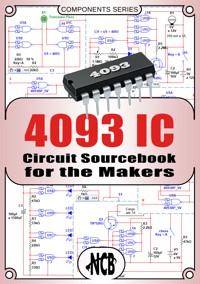
4093 IC - Circuit Sourcebook for the Makers
Institute NCB
www.newtoncbraga.com
4093 IC - Circuit Sourcebook for the MakersAuthor: Newton C. BragaSão Paulo - Brazil – 2017
key-words: Electronic, IC, 4093, Maker, Circuit, shield
Officer responsible: Newton C. Braga
Design and Coordination: Renato Paiotti
More Information
INSTITUTe NEWTON C. BRAGA
http://www.newtoncbraga.com
NOTA IMPORTANTE
Esta série de livros fornece conhecimentos básicos de eletrônica para cursos regulares, cursos a distância e para autodidatas consistindo, portanto numa literatura cuja finalidade é apoio, iniciação ou complementação de conhecimentos. Sua aquisição não implica no direito a obtenção de certificados ou diplomas os quais devem ser emitidos pelas instituições que adotam o livro ou ainda ministram cursos de outras formas. Da mesma forma o autor ou a editora não se responsabilizam por eventuais problemas que possam ser causados pelo uso indevido das informações nele contidas como o não funcionamento de projetos, ferimentos ou danos causados a terceiros de forma acidental ou proposital, ou ainda prejuízos de ordem moral ou financeira. Os eventuais experimentos citados quando realizados por menores devem ter sempre a supervisão de um adulto. Todo cuidado foi tomado para que o material utilizado seja encontrado com facilidade na época da edição do livro, mas as mudanças tecnológicas são muito rápidas o que nos leva a não nos responsabilizarmos pela eventual dificuldade em se obter componentes para os experimentos quando indicados em outros livros desta série.
Índice
Presentation of the New Edition
Preface
Cover of the original version (1999)
Sources for the 4093
Chapter 1 - The 4093 CMOS IC
1.1 The CMOS Family
1.2 The 4093 IC
1.3 Basic Configurations
1.4 Power Supplies
Chapter 2 - Audio and RF Projects
Project 1 - Simple Audio Oscillator (E) (P) (S)
Project 2 - Simple Audio Oscillator II (E) (P) (S)
Project 3 - Signal Injector (P) (E)
Project 4 - Touch-Controlled Oscillator (E)
Project 5 - Touch Switch Shield (S)
Project 6 – Light-Controlled Oscillator I (E) (P) (S)
Project 7 - Plasma Oscillator (E) (S)
Project 8 - Insect Repellent (P)
Project 9 - Audio Generator (P)
Project 10 – Metronome I (E) (P)
Project 11 – Metronome II (E) (P)
Project 12 – Ultrasonic Generator I (E) (P) (S)
Project 13 - Ultrasonic Generator II (E) (P) (S)
Project 14 – Ultrasonic Generator III (E) (P) (S)
Project 15 - High Power Ultrasonic Generator (E) (P) (S)
Project 16 - Match Oscillator (E)
Project 17 - Morse Code Tone Generator (P) (E) (S)
Project 18 – 100 Hz to 1 kHz Oscillator (P) (E) (S)
Project 19 - Touch-Controlled Oscillator II (E) (P) (S)
Project 20 - Light Controlled Oscillator (E) (P) (S)
Project 21 - 100 kHz to 1 MHz CW Transmitter (E)
Project 22 - Modulated 100 kHz to 1 MHz Transmitter (E)
Project 23 - 3 to 4 MHz CW Transmitter (E)
Project 24 - Tone Modulated 3 to 4 MHz Transmitter (E) (S)
Project 25 – Beeper (E) (P) (S)
Project 26 - Power Beeper (E) (P) (S)
Project 27 - Beeper (version III) (E) (P) (S)
Project 28 - Two Tone Beeper (E) (P) (S)
Project 29 – Power Beeper IV (E) (P) (S)
Project 30 - Complementary Beeper (E) (P) (S)
Project 31 - Two-Tone Siren (P) (S)
Project 32 - Frequency Modulated Siren (P) (S)
Project 33 - Complex Sound Generator (E) (P) (S)
Project 34 - Variable Interval Beeper (E) (P) (S)
Project 35 - Variable Duty Cycle Siren (E) (P) (S)
Project 36 - Touch Triggered Siren (E) (P)
Project 37 - Sound Machine (E) (P)
Chapter 3 - Lamp and LEDs Projects
Project 38 - Simple LED Flasher (E) (P) (S)
Project 39 - 4093 IC Tester (P)
Project 40 - 6/12 V Incandescent Lamp Flasher (P) (S)
Project 41 - Variable Duty Cycle Incandescent lamp Flasher (E) (P) (S)
Project 42 - Flasher with Beeper (E) (P) (S)
Project 43 - Simple LED Flasher II (E) (P) (S)
Project 44 - Dual Variable Duty Cycle Flasher (E) (P) (S)
Project 45 - Dual LED Flasher (E) (P) (S)
Project 46 - Complementary Transistor Dual LED Flasher (E) (P) (S)
Project 47 - Two Color LED Flasher III (E) (P) (S)
Project 48 – Dual High Power Flasher (E) (P) (S)
Project 49 - Delayed Turn-Off Lamp (E) (P) (S)
Project 50 - Neon-Lamp Flasher (E) (P)
Project 51 - Delayed Turn-Off Flasher (E) (P)
Project 52 - Touch-Triggered LED-Flasher (E) (P)
Project 53 - Variable Duty Cycle Lamp Flasher (P) (S)
Project 54 - Dark-Activated Lamp Flasher (P)
Project 55 - Variable Duty Cycle Flasher (E) (P) (S)
Chapter 4 - Time-Delay Projects
Project 56 - Simplest Timer (E) (P)
Project 57 - Auto Turn-Off Relay (P)
Project 58 - Simple Timer II (P)
Project 59 - Continuous Sound Output Timer (E) (P)
Project 60 - Pulsed-Tone Timer (E) (P)
Project 61 - Turn On-Off Timer (E) (P)
Project 62 - Pulsed Tone Turn-Off Timer (E) (P)
Project 63 - Dual Turn-On Timer (E) (P)
Project 64 - Turn On and Off Timer (E) (P)
Project 65 - Turn On and Turn-Off Timer (E) (P)
Project 66 - Turn On and Off Timer with Relay (E) (P)
Project 67 - Dual Mini-Timer (E) (P)
Project 68 - Dual Pulsed Tone Timer (E) (P)
Project 69 - Four-LED Bargraph Timer (E) (P)
Project 70 - Bargraph and Relay Timer (E) (P)
Project 71 - Incandescent Lamp Timer (P)
Project 72 - Incandescent Lamp Dual Timer (P)
Project 73 - Automatic Turn-On and Turn-Off Timer (P)
Chapter 5 - Bistable Circuits
Project 74 - Touch Activated Bistable (E) (P) (S)
Project 75 - Touch Turn On and Off Relay (E) (P) (S)
Project 76 - Touched Controlled Motor (E) (P) (S)
Project 77 - Unilateral Counter (E) (P) (S)
Project 78 - Bistable Sonic Relay (E) (P) (S)
Project 79 – Bistable II (E) (P) (S)
Project 80 - Touch-Activated Relay II (E) (P) (S)
Project 81 - Bistable Light Remote Control (P) (S)
Project 82 - Coin Tosser (P)
Chapter 6 - Alarms
Project 83 - Swimming Pool or Rain Alarm (P)
Project 84 - Pendulum Intermitent Alarm (P)
Project 85 - General Purpose Remote Alarm (P)
Project 86 - Bistable Light Alarm (P)
Project 87 - Freezer Alarm (P)
Project 88 - Bistable Remote Control (P)
Project 89 - Delayed Turn-On Alarm (P)
Project 90 - Delayed Turn-On Alarm (version II) (P)
Project 91 - Delayed Alarm (P)
Project 92 - Burglar Alarm Center (P)
Project 93 - Under Temperature Alarm (E) (P)
Project 94 - Under-Temperature Relay (E) (P)
Project 95 - Over-Temperature NTC Relay (E) (P)
Project 96 - Timed Pendulum Alarm (E) (P)
Chapter 7 - Inverters
Project 97 - Simple Fluorescent Lamp lnverter (E) (P) (S)
Project 98 - Ultraviolet Lamp (E) (P) (S)
Project 99 - Experimental High Voltage Generator (E) (P)
Project 100 - Nerve Stimulator (E) (P)
Project 101 - Dark-Activated Fluorescent Lamp-Flasher (P) (E)
Project 102 - Light Activated Lamp Flasher (E) (P)
Project 103 - Fluorescent Lamp Flasher (E) (P) (S)
Project 104 - Negative Ion Generator (E) (P)
Project 105 - Fluorescent Strobe Light (E) (P) (S)
Part 8 - Miscellaneous Projects
Project 106 - Gated Oscillator – version I(E) (P) (S)
Project 107 - Gated Oscillator – version II (E) (P) (S)
Project 108 - 60 Hz Generator (E) (P) (S)
Project 109 - Electroscope (E) (P)
Project 110 - Modulated Generator (P)
Project 111 - Capacitor Tester (P)
Project 112 - X-Ray Detector (P)
Project 113 - Continuity Tester (P)
Project 114 - Auditory Capacitor Tester (P)
Project 115 - Fixed-Tone Continuity Tester (P)
Project 116 - Time Delayed Generator (P) (S)
Project 117 - Time-Delayed Generator II (P) (S)
Project 118 – Dexterity Tester (P)
Project 119 - Water Sensor (P) (S)
Project 120 - Electronic Organ (E) (P)
Project 121 - Electronic Organ with Vibrato (E) (P)
Project 122 - Sound Activated LED or Relay (E) (P) (S)
Project 123 - Simple Bargraph (E) (P)
Project 124 - General Purpose Automatic Switch (E) (P)
Project 125 - Dark-Activated Flasher (E) (P)
Project 126 - Touch Switch (E) (P)
Project 127 - High Power Touch Switch (P)
Project 128 - Optocoupler Interface or Shield (P) (S)
Project 129 - Twin Lamp AC Flasher (P)
Project 130 - Flickering Flame Effect (P)
Project 131 - Dark-Activated Lamp (P)
Project 132 - Power Bistable with Magnetic Switches (P)
Project 133 - AC Lamp Flasher (P)
Project 134 - Full Wave Touch Switch for AC Loads (P)
Presentation of the New Edition
In 1999 we published a book on the CMOS integrated circuit 4093, an edition in English only for Newnes who was named CMOS Projects and Experiments - Fun with the IC 4093, which was a great success, meeting today totally exhausted. The publication describing 135 projects using CMOS integrated circuit 4093, selected from my vast collection, was published in Brazil earlier in the form of articles and isolated circuits. The publication ran out, had their Portuguese version so far, but the 4093 circuit remains more relevant than ever. With the advent of microcontrollers and the new philosophy of the “makers”and the STEAMERs, or projects doers with many different purposes, the 4093 again proved to be extremely useful, whether for independent assemblies, as well as shields for microcontrollers. So checking the need for a publication with projects using the 4093, also useful for teachers and students, we review that book and with many upgrades made an English version soon will also be translated into Spanish. This new edition brings a more modern approach for the 4093 with suggestions for shields and breakout boards, as well as applications that were not possible at the time of its first release. It is, therefore, a new book with a new approach to one of the most useful integrated circuits that we know. As far as the 4017 and the 555, the 4093 should be considered an essential component in the bench throughout makers, experimenters, teachers or students.
Preface
Some special components, such as the 555, 741, 567, 4017, and other popular ICS, can be used as the basis of a large assortment of electronics projects. The 4093 CMOS is one of these components. Using this versatile IC, the author compiled this special “one-component cook-book” that furnishes the experimenter, “maker”, student, and technician with a large selection of practical circuits.
During the past several years, the author, as a contributor to U.S., European, and Latin American electronics magazines, has collected a large assortment of electronic projects using the 4093 CMOS IC. Practical circuits, as well as ones that can teach you a great deal about electronics or be part or of a microcontrolled project as shield, have been selected and included in this book.
This book has a dual aim, as we have two kinds of electronics experimenters: (1) those who want to improve or expand their understanding of some other areas of interest, such as audio, radio, microcontrollers, instrumentation, security, or even games, and (2) those who want to gain an understanding of basic electronic circuits and the 4093 CMOS IC, which is the basis of this work. Both are “makers” that want to do something new with this component, using them alone in a complete application or as part of a shield or breakout board in a project with microncontrollers.
We should also mention another kind of reader: the high school student who wants to use electronics in scientific explorations The STEAMer. Many projects described in this book can be used in scientific experiments or middle school science projects.
Most of the projects described here can stand alone as individual devices. However, wherever possible, the circuits have been designed so they can be ganged with one or more other projects as a shield or breakout board for microcontrollers. For example, many projects of audio effects and sound generators can be joined with the audio output stages outlined herein to drive several types of loads ranging from low-power piezoelectric transducers to high-power loudspeakers.
They can also be controlled by the outputs of a microcontroller acting as sound effects, motor controls, or other king of shield in many projects.
We also have simple projects that use only a few low-cost components. These can be assembled in a single evening even in a class using a solderless board, as opposed to the more complicated projects that employ several ICs, transistors, and other parts. To make it easier for the reader to choose appropriate projects, each project title is labeled with a “P” to indicate that it has practical uses, an “E” to indicate that it is designed for the experimenter to teach him something about circuits or devices or a “S’ to indicate that it can be used as shield. You will find also projects with both marks (E and P), and these can be used for either purpose.
Chapter 1 describes, in simple terms, the 4093 IC itself. After this brief introduction, the remaining chapter provides 135 projects in a straightforward manner, grouped by general types. It begins with simpler projects and progresses to the more complex. This format should enable the reader to learn the theory of the device quickly and prepare him to use the circuits most advantageously. The projects also have informations that allow their use as shield in projects using microcontrollers such as the Arduino, PIC and others.
The required electronic components are listed with each circuit diagram. Secondary parts as sockets, chassis, enclosures, miscellaneous hardware, and so on are not specified, since the reader is free to choose these non-critical items according to his preference and demands.
The manner in which the circuits work, and acceptable modifications, are explained in practical terms so the reader can acquire additional knowledge of practical electronics as he progresses through the book.
Although many of the projects (the practical ones) are fun to build exactly as they are discussed here, you may think of possible modifications. I recommend that you go ahead and modify the circuits to suit your personal ends. There is wide latitude for circuit modifications, and most of them will be of value to experimenters who want to see how things work, even though each project,s primary value is for the builder who wants to produce a practical, functional item.
Because our projects utilize a wide range of power supply voltages, we have included several different regulated and unregulated power supply projects so that the reader doesn,t run up an expensive bill for batteries. In applications where the 4093 is used with microcontrollers, how to power them from the microcontroller’s board is explained.
The power supply requirements of each project have been tailored to one or more standard voltages that cam be easily attained using commonly available batteries or power supply transformers. The voltage, in most instances, will be similar to those for projects described in the author’s site (www.newtoncbraga.com), so a power supply from this book can also be used for many projects from other sources. (*)
We also recommend visit the author’s site where many other projects using the 4093 IC can be found. There, can be also found in the section “Simulated Circuits” the simulation in the Multisim software with files that can be directly be downloaded to ypour computer or laptop.
As a whole, I believe this book will serve a definite purpose and fill a possible void in your repertoire of exciting electronic items.
Newton C. Braga
(*) Also site em Spanish (www.incb.com.mx) and Portuguese (www.newtoncbraga.com.br)
Cover of the original version (1999)
This is the cover of the edition published by Newnes in 1999, today na out.
Sources for the 4093
The 4093 integrated circuit can be purchased from many dealers. The reader can visit the site of the author and acces the tool to find electronic parts in the Internet the site of Mouser Electronics or directly at www.mouser.com . Only take care to choos the DIL version of the IC since the SMD cannot be used with solderless boards.
In addition, you can find sources for most components on your local dealer since the 4093 is a very comon IC.
Chapter 1 - The 4093 CMOS IC
1.1 The CMOS Family
The 4093 CMOS integrated circuit is a member of a large group of compatible building blocks. With these blocks, we can build circuits that make simple decisions, so they are also classiiied as digital logic circuits. The CMOS group of integrated circuits is composed of several types of devices that, because they have the same input/output electrical characteristics, can be interconnected without the need of intermediate circuitry. They can be conncted directly to the input or output of microcontrollers making then very useful to build shields or breakout boards.
There are many digital logic families available as TTL (transistor-transistor logic), RTL (resistor-transistor logic – not used today), and others, but the 4093 IC is a member of the CMOS (complementary metal-oxide-silicon) family, which has some important advantages over other families. These benefits include very low cost; ultra-low, noncritical power requirements; and an ultra-high input impedance.
These features, plus the inherent advantages of CMOS ICs over other logic devices, permit the logic system designer/experimenter to achieve outstanding electrical performance, high reliability, and simplified circuitry in a wide variety of equipment designs.
Some CMOS features are as follows:
All devices inputs are open circuits and thus are easy to drive.
They will run on ultra-low operating currents, particularly at low frequencies.
They have high noise immunity-typically, 45 percent of supply voltage.
They operate in a wide voltage range: 3 to 15 V (A-series devices) and 3 to 18 V (B-series devices).
The inputs are fully protected.
They feature large unloaded output swing: the output goes from ground potential (0 V) to the positive supply.
They generate very little noise in power supply lines.
The manner in which CMOS integrated circuits are fabricated and the characteristics of all families can be found in several specialized books, normally classified as “digital electronics books,” and in articles published in electronics magazines and sites in the internet, such as the author’s (www.newtoncbraga.com). If the reader wants more information about CMOS family, and digital electronics in general before to starting with our projects, a brief look in such sources might be valuable.
1.2 The 4093 IC
The 4093 CMOS integrated circuit is formed by four two-input NAND Schmitt triggers in a 14-pin package. All four positive-logic NAND gates may be used independently (Fig. 1).
Figure 1 – 4093 CMOS IC, functional diagram.It is avaliable in 14-pin dual in-line (DIP) package.
Other packages re used such as the SMD, micro and plastic carrier, but to work in a solderless board or make common building using printed circuit boards the DIP is the recommended.
In Fig. 1, we show the package used for this IC and also the NAND symnbol and Schmitt trigger symbol. In terms of logic, the action of the circuit is the same as the action of the common NAND gate. The figure also shows the truth table for the gate.
The output logic level depends on the input logic level. A zero appears at its outputs if both inputs are ones, and a one appears at its output if either or both inputs are zeros.
We should remind the reader that a zero (or a low legic level) is given by a 0-volt voltage, and a one (or high logic level) is given by the positive supply voltage-also called +Vcc or Vdd.
For the 4093 IC, and all devices of CMOS logic family, +Vcc, or the positive supply, can range from +3 to +15 V (A-series devices) or +3 to +18 V (B-series devices). For circuits that operate in a linear mode over a portion of the voltage range, such as RC or crystal oscillators, a minimum supply voltage of 4 V is recommended (In this book more parte of the projects will operate in the range between 3 and 12 V).
The difference between a common NAND gate and a Schmitt NAND gate is the snap action with hysteresis that it provides, also called dead band. Let,s explain:
In Figure 2, we show the transfer characteristic of a 4093 ICS Schmitt trigger. The general shape of this characteristic is the same for all values of Vdd (positive supply) until Vp is reached.
Figure 2 – Transfer characteristic of the 4093. The difference between Vp and Vn is called hysteresis voltage.
At this point, the output goes low (0 V) and remains low as the input voltage is raised to Vdd. If the input voltage now is reduced, the output goes high and remains high as the input voltage is reduced to zero.
The hysteresis is the difference between Vp and Vn, which is typically 0.6 V for a 5.0 Vs power supply.
Figure 3 shows the input/output characteristic of a 4093 device. Note that Schmitt triggers are bistable circuits that are driven by their inputs. They are useful for squaring up slowly rising or noisy inputs, contact debouncing, and oscillators. We can conclude that the 4093 offers unlimited possibilities for the experimenter, and in the following pages we show many of them. The reader, having a large imagination, can explore the basic circuits and get much more from them.
Figure 3 – Input and output characteristics of the 4093 IC
1.2.1 – Circuits simulatation using the MultiSIM
Each simulation program adopts a certain type of representation, even if the symbols of the components have a pattern, the way they are inserted in these programs varies from program to program. We use the MultiSIM version 14 Educational Edition in this book, and for this reason it is important for the reader to understand how the 4093 appears. Because the 4093 is made up of 4 NAND ports, when you enter them on the screen, the program does this by using the letters A, B, C, and D for each NAND port.
In the case of the schemes presented in this book which were simulated in the MultiSIM, the reader should bear in mind that U1A represent pins “1”, “2” (inputs) and “3” output; The pins “5”, “6” (inputs) and “4” output; The pins “8”, “9” (inputs) and “10” output; The pins “12”, “13” (inputs) and “11” output. In the simulated diagramse in this book, we added as a didactic reference pins 7 and 14, because in the MultiSIM, when we added the 4093, it automatically already makes the connections to these two pins (Power and Earth). In the simulation we observed that there is a difference between what we show in the drawing and the actual simulation in some cases. For example, in some circuits where a speaker or piezoelectric transducer appears on the output, there is no sound in the simulation, because Multisim does not always have these features available. To simulate the operation we connect the output to the input of an oscilloscope to verify the presence of the desired audio signal.
Another possibility is to connect the external speaker box that some versions have and allow you to use the sound of the multimedia system.In our case, at the end of each article that has the simulation, we will give instructions on how to do it.
1.3 Basic Configurations
1.3.1 NAND Schmitt Trigger
Of course, the basic internal circuit of the 4093 is designed to be a NAND gate and therefore to operate as a logic unit that makes some simple decisions given by the table in Fig. 1. Accordingly, the basic application of this device is as a NAND gate.
The ultra-high input impedance of the device, typically 1012 ohm, allows the utilization of large input resistors in a circuit such as the one given in Fig. 4.
Figura 4 – The 4093 used as NAND Gates controlled by SPST switches
As we also see in that ligure, the input voltage determines the output voltage in four possible conditions. We will use this basic configuration in several projects.
The maximum output current of each gate depends on the power-supply voltage, and at 25º C they are as follows:
Vdd (V)
Max. current (sink and source) (mA)
5 V
01/01/00
10 V
02/06/16
15 V
06/08/16
1.3.2 Inverter
The simplest possible logic block has one input and one output. We can make this simple block with the 4093 Schmitt triggers by wiring one of the two inputs to the positive supply (Vdd) or wiring the two inputs together as shown in Fig. 5
Figure 5 –The 4093 wired as an inverter
One input of this block can be used for control in shields. In this case the 4093 is powered from the microcontroller source (3.3 or 5 V) and the gate is enable by a High (1) logic level at the control input.
The truth-tables in Fig. 5 show that, when the input is a one, the output is a zero, and vice versa. The block inverts the logic level applied to its input and so is called an inverter.
Inverters are used to generate the complement of a logic signal or to change the definition of a logic signal from positive to negative and back again. Remember that in digital logic, the complement of 0 is 1, and the complement of 1 is 0.
To indicate that the block changes the signal, we use a small circle in its symbol output. In Fig. 6, we show how to use this circuit as a rise-time enhancer. Extremely slow signals or ultra-low frequency sinewaves can be converted to fast-rise outputs in this way.
Figure 6 – The 4093 wired as an inverter
The same configuration can be used to eliminate noise on a system input, as shown in Fig. 7. Note that, for complete rejection, the noise amplitude can be less than the dead band.
Figure 7 – The 4093 as a noise eliminator
Contact debouncers or conditioners are shown in Fig. 8, based on a 4093 Schmitt trigger. The contacts debouncers are conceived for normally open and normally closed single switches, and these circuits operate by discharging or recharging a RC network. For best performance, the RC network time constant must exceeds three times the worst-case bounce time. Depending on the power-supply voltage, the 4093 will operate from dc to 1 MHZ in this application.
Figure 8 – Normally open and normally closed contact debouncers
1.3.3 Oscillator
Stable oscillators may be constructed easily using the 4093 NAND gates. Figure 9 shows the basic circuit and its waveforms. It works as follows:
Figure 9 – Basic NAND gate oscillator with the output waveform.The period is given by the formula.
Before power is applied, input and outputs are at the ground potential (0 V, or logic level 0) and capacitor C is discharged. At power on, the output goes to high (Vdd, or logic level 1), and C charges through R until Vp is reached. The output then goes low. C is now discharged through R until Vn is reached. The output then goes high and charges C toward Vp through R. Therefore, we conclude that input alternatively swings between Vp and Vn as the output goes high and low.
An important advantage of this circuit is that the oscillator is self-starting at power on. We also see that the basic oscillator consists of an amplifler (4093 gate) and a feedback network. For oscillation to occur, the gain of the amplifier x attenuation of the feedback network must be greater than 1.
The frequency stability of an oscillator such as this is primarily dependent on the phase-changing properties of the feedback network. For the 4093, we have good performance in frequencies as high as 1 MHz, and the RC network values are given in the figure.
As in the case of inverters, the oscillator can be controlled by one input, allowing the operation as shield. In this case the 4093 must be powered from the microcontroller’s voltage source and the oscillator is enabled by a high (1) logic level at the control input.
Many projects in this book will use this configuration. See item 1.3.8.
1.3.4 Monostable Multivibrator
The monostable multivibrator has one stable state and one unstable state. It remains in the stable state until it is triggered. When triggered, it will be placed temporary in the other state. The multivibrator will remain in that state during a time delay, after which it snaps back to its original condition.
We can use monostable multivibrators to detect leading and trailing edges of waveforms, in medium-accuracy generators, and also in time-delay generators.
Each gate of a 4093 IC can be used as monostable multivibrator. There are several ways to create a monostable multivibrator with the gates as shown in Fig. 10.
Figure 10 – monostable circuits with the 4093
In Fig. 10a, we show a positive-edge responding monostable multivibrator. In this configuration, the output goes to 0 during a definite time delay given by the RC network, and it swings back to 1 when a positive transition occurs in its input.
In Fig. 10b, a negative-edge responding coniiguration is shown. The output swings from zero to one during a definite time delay when the input voltage falls from one (+Vcc) to zero (0 V).
This circuit can be controlled by microcontrollers acting as a shield in many applications. (See item 1.3.8)
Resistor values in the RC network can go from 10 k up to 10 M, and the capacitor can range from 50 pF on up.
Time delay as function of component values in the RC network is given in the chart shown in Fig. 11. Some usage limits should be observed for this kind of monostable multivibrator:
Figure 11 – Component values for monostable operation
The input voltage must stay in the post-trigger state for a period of time longer than the on time. The input transition must be noise free. The circuit may not be retriggered until after full recovery. The input must return into the pretrigger state long enough to let the RC network recover fully.
As, really, the circuits shown are edge detectors, they also can be called half monostable.
1.3.5 Set-Reset Flip-Flop
In Fig. 12 we show how two NAND gates of a 4093 can be wired to form a set-reset flip-flop. The circuit is a pulse-triggered flip-flop that needs a negative-moving pulse to be triggered.
Figura 12 – Set-Reset flip-flop using two-gates of a 4093 IC
This circuit operates as follows.
As we can see, the circuit has two outputs: a normal output, called Q, and a inverted output called Q\. When one output is 1, the other necessarily will be a 0, and vice-versa, because they are complementary.
The circuit has also two inputs named S (set) and R (reset), as shown in the figure, where the trigger signals are applied. R input is wired to Q output, and S input is wired to Q\ output, performing a closed-loop for the digital signals.
When a negative-moving trigger pulse is applied to S input, the output Q swings to the 1 state. As this output is wired to input R, the 1 state causes output Q\ to fall to a 0 level. But Q output is also wired to input S, causing a feedback that causes its output to remain at 1 even after the trigger pulse has disappeared.
To trigger the multivibrator again, changing the output states, we should apply a negative-moving pulse to input R. This pulse causes the output to go 1 and, as this input is wired to input R, the trigger pulse also causes the output Q to go to a 0 level.
A zero in this output Q goes to input S and also, after the trigger pulse disappears, the outputs remain in their states. Note that the circuit has two stable states, and we only can change these states with set or reset (R or S) negative-moving pulses applied to its inputs. A manually triggered flip-flop can be constructed by wiring switches to the set-reset inputs as shown in Fig. 13.
Figure 13 – Manually triggered flip-flop using two gates of a 4093 IC
The 4093 high input impedance allows the use of a large range of resistor values in this application. They typically can range from 1 k to 10 M. Resistors are used to apply a high logic level at the inputs when the switches are open. Without the resistors, we will have an indefinite state at the inputs when the switches are off, and this could cause erratic operation of the circuit. With high-value resistors in this circuit we can get a touch-triggered bistable as shown in Fig. 14.
Figure 14 – Touch controlled flip-flop using two gates of a 4093
Many projects in this book use that configuration as the starting point. We can obtain different performances for this basic circuit using other gates as inverters and obtain positive-moving bistables.
This ciruit can also be used in shield (see previous configurations).
1.3.6 Two-Gate Oscillator
Two NAND Schmitt triggers of a 4093 can create a two-gate oscillator, as shown in Fig. 15. This circuit generates a square wave with excellent thermal stability and operates in a large range of frequencies. With the values shown in Fig. 15, it operates at about 1 kHz.
Figure 15 – Two- gate oscillator runing at 1 kHz
In practice, C1 must be a nonpolarized capacitor and can have any value from 50 pF to some microfarads. R1 can have any value in the range between 4.7 k and 20 M. As in other applications, for a variable frequency operation, Wire a fixed and a variable resistor in series in the R1 position.
The voltage in the junction of C1 and R1 is prevented from swing below zero or above the positive supply level by the built-in clamping diodes at the 4093 inputs, which causes the operating frequency of the circuit to be somewhat dependent on the power supply voltage. A simple rule shows that the frequency falls about 0.1 percent for each 1 percent rise in supply voltage.


