106,99 €
Mehr erfahren.
- Herausgeber: Wiley-VCH GmbH
- Kategorie: Fachliteratur
- Sprache: Englisch
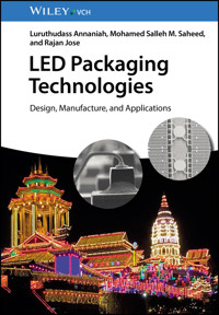
LED Packaging Technologies
Up-to-date practitioner’s guide on LED packaging technologies, with application examples from relevant industries, historical insight, and outlook
LED Packaging Technologies provides expert insight into current and future trends in LED packaging technologies, discussing the fundamentals of LED packaging technologies, from electrical contact design, thermal management and optical emission, and extraction, to manufacturing technologies, including the JEDEC testing standards, followed by accounts on the main applications of these LED packages in the automotive, consumer electronics, and lighting industries.
LED Packaging Technologies includes information on:
- History of primitive lighting in human civilization to the invention of modern LEDs based lighting, and historic evolution of LED packaging technology
- Basic light emission and extraction technology in LED packages, covering package design impacting light emission and extraction
- Medical industry applications of LEDs, especially in healthcare treatments, such as in skin rejuvenation and wound healing and closures
- Quantum confinement phenomena and size-dependent optical properties of quantum dots, and the advancement of future quantum dot LEDs
Covering the fundamentals, design, and manufacturing of LED packaging technology and assisting in removing some of the barriers in the development of LED packaging and new applications, LED Packaging Technologies is an essential source of information for engineers in the LED and lighting industries, as well as researchers in academia.
Sie lesen das E-Book in den Legimi-Apps auf:
Seitenzahl: 291
Veröffentlichungsjahr: 2023
Ähnliche
Table of Contents
Cover
Title Page
Copyright
About the Authors
Preface
Acknowledgments
1 A Brief History of Artificial Light and LED Packaging
1.1 Evolution in Artificial Light
1.2 Impact of Light‐Emitting Diode on the World
1.3 LED Industrial Chain
1.4 Evolution in LED Packaging Technology
1.5 Summary
References
2 Fundamentals of LED Packaging Technology
2.1 Effective Light Extraction
2.2 Package Design and Encapsulation Technology
2.3 LED Thermal Management
2.4 Electrical Contact Design
2.5 LED Light Conversion Principle
2.6 Summary
References
3 LED Packaging Manufacturing Technology
3.1 LED Packaging Process Flow
3.2 Common Defects in LED Packaging Industry
3.3 Summary
References
4 LED Automotive Lighting Application Technology
4.1 Basic Science of Light for Automotive – The Photometric
4.2 Lighting – Light Projection “To See”
4.3 Signaling – Lights That Are “To Be Seen”
4.4 Interior Lighting
4.5 Summary
References
5 LED Application For Consumer Industry
5.1 Consumer Indoor Lighting
5.2 Health Care and Medical Treatments
5.3 Safety and Security
References
6 LED Application for General Lighting
6.1 RETROFIT Lighting
6.2 LEDfit Lighting
6.3 Summary
References
7 Quantum LEDs
7.1 Quantum LED as the Alternative to Organic LED
7.2 Fundamentals of Quantum Dot
7.3 Quantum Dots in LED
7.4 Quantum LED Structures
7.5 QD‐LED Fabrication
References
8 Ultraviolet LED Packaging and Application
8.1 UV LED Application
8.2 UV‐A and B LED Packaging Technology
8.3 UV‐C Packaging Technology
8.4 Future Application of UV‐LED and Packaging Design Evolution
8.5 Impact of UV‐LED to UV Light Source Business
8.6 Summary
References
9 Lifecycle Analysis and Circular Economy of LEDs
9.1 Introduction
9.2 LCA of LEDs
9.3 Circular Economy of LEDs
References
Index
End User License Agreement
List of Tables
Chapter 1
Table 1.1 Potential impact of conversion to solid‐state lighting on U.S. ele...
Table 1.2 General description of low‐, mid‐, high‐, and ultra‐high‐power LED...
Chapter 3
Table 3.1 Moisture sensitivity level and the requirement for packing.
Chapter 4
Table 4.1 European Commission regulation for automotive lighting systems.
Chapter 8
Table 8.1 The advantages and disadvantages of UV LEDs and UV lamps.
Chapter 9
Table 9.1 Weight of various components used in a single LED.
Table 9.2 Weight of various components used in a single LED to reduce the ma...
List of Illustrations
Chapter 1
Figure 1.1 Evolution of artificial light.
Figure 1.2 Solid‐state lighting expanding application. Source: Courtesy of a...
Figure 1.3 LED industrial chain. Source: Courtesy of ams OSRAM GmbH.
Figure 1.4 (a) AlInGaN chip top view showing current spreader, (b) AlInGaN c...
Figure 1.5 LED package evolution. Source: Courtesy of ams OSRAM GmbH.
Figure 1.6 Illustrate a standard surface mount LED package. Source: Courtesy...
Figure 1.7 High‐power packages: (a) Golden DRAGON package, (b) Golden DRAGON...
Figure 1.8 Radial package in a cross‐section view.
Figure 1.9 Some of the mid‐power LED packages. Source: Courtesy of ams OSRAM...
Figure 1.10 Mid‐power LED PLCC package thermal management design evolution....
Figure 1.11 High‐power LED packages with a variety of solutions. Source: Cou...
Figure 1.12 High‐power LED PLCC package thermal management design: (a) Golde...
Figure 1.13 High‐power LED package construction. Source: Courtesy of ams OSR...
Chapter 2
Figure 2.1 LED converts electrical energy into light. Source: Courtesy of am...
Figure 2.2 LED p–n junction in forward bias. Recombination occurs in the dep...
Figure 2.3 p–n junction under the forward bias conditions, minority carriers...
Figure 2.4 Light paths in GaN/sapphire chip.
Figure 2.5 Solid angle escape cone. Dark line indicates the critical angle f...
Figure 2.6 Buried micro‐reflectors showing emission regions of the LED. Sour...
Figure 2.7 (a) Optical microscopy images of various LED chips with various g...
Figure 2.8 Light emission of the standard Top Emitter chip vs Volume Emitter...
Figure 2.9 Light emission of the Flip chip Thinfilm vs Volume Emitter chip. ...
Figure 2.10 LED packaging that can be used for Thinfilm, Flip chip, and Volu...
Figure 2.11 The lead frame plating surface finishing and light reflection. (...
Figure 2.12 Injection‐molded leadframe and OSRAM TopLED PLCC package. Source...
Figure 2.13 Optical properties of encapsulation material.
Figure 2.14 Schematic diagram of (a) CSP package, (b) SMD package, (c) FDCSP...
Figure 2.15 Light‐tracing profiles of (a) CSP: 1.5 mm × 1.5 mm × 0.8 mm, (b)...
Figure 2.16 LED package external contact pin surface quality affecting testi...
Figure 2.17 (a) CSP lead contacts and (b) recommended PCB solder pad design....
Figure 2.18 LED epoxy package turned dark after prolonged exposure to blue l...
Figure 2.19 Mechanical properties of encapsulant materials. Source: Denko [1...
Figure 2.20 Metal can package. Source: Courtesy of ams OSRAM GmbH.
Figure 2.21 OSRAM Butterfly package for Laser project application. Source: C...
Figure 2.22 Epoxy cap encapsulation package. (a) Lens attached on the pre‐mo...
Figure 2.23 ams OSRAM's new glass‐encapsulated UV LED. Source: Courtesy of a...
Figure 2.24 p–n junction under the forward bias conditions, minority carrier...
Figure 2.25 The basic LED construction with an equivalent circuit diagram of...
Figure 2.26 The electrical and thermal transient processes occurred during t...
Figure 2.27 Shows OSRAM Golden Dragon package's thermal performance.
Figure 2.28 Conduction heat path in the LED die. It passes through the chip ...
Figure 2.29 A comparison of thermal path and thermal resistance between low‐...
Figure 2.30 The internal and external electrical contact in the LED package....
Figure 2.31 (a) Remote phosphor distribution of two‐flat phosphor geometry i...
Chapter 3
Figure 3.1 LED packaging process flow.
Figure 3.2 Die‐attach process: (a) ceramic printed substrate, (b) die‐attach...
Figure 3.3 Small LED chip bondline thickness and glue (silver) height. Sourc...
Figure 3.4 Gold wire against fussing current.
Figure 3.5 Gold wire bonding on sapphire chip. Source: Courtesy of ams OSRAM...
Figure 3.6 (a) Heat‐affected zone (HAZ) of gold wire Source: Image from Hera...
Figure 3.7 (a) Dage Tester, (b) the shear tool, (c) the wire pull tool, and ...
Figure 3.8 Surveillance checking, (a) glue remnant on the substrate. (b) gol...
Figure 3.9 (a) Mold design with lens, (b) Transfer Molding equipment. (b) Th...
Figure 3.10 (a) Sawing process conceptual diagram. (b) Singulation blades gr...
Figure 3.11 (a) An industrial‐grade test handler with electro‐optical tester...
Figure 3.12 (a) Moisture‐sensitive product is packed in a dry bag containing...
Figure 3.13 Current–voltage (
I
–
V
) curves for the selected fractured dice and...
Figure 3.14 Die cracked LED biased with low current, showing a dimming affec...
Figure 3.15 (a) Lifted glue LED failure X‐ray photo, (b) lifted die LED fail...
Figure 3.16 (a) Lifted ball, (b) cratering die bond pad, (c) broken wire/sti...
Chapter 4
Figure 4.1 Automotive lighting system that shows various lights that cover l...
Figure 4.2 Radiation pattern of an LED – OSLONSX – LA CN5M. Source: Courtesy...
Figure 4.3 Spectral sensitivity of human eyes. Source: Courtesy of ams OSRAM...
Figure 4.4 (a) General description of a low‐beam lamp on a road, (b) low‐bea...
Figure 4.5 General description of (a) high‐beam lamp on the road, (b) high‐b...
Figure 4.6 General description of (a) fog beam lamp on the road, (b) fog lam...
Figure 4.7 Evolution of adaptive front light system.
Figure 4.8 Dynamic auto‐leveling headlamp system. Source: Kobayashi [11], SA...
Figure 4.9 Headlamp comparison between the Conventional System and Matrix LE...
Figure 4.10 Matrix LED headlights. Source: Image from FORVIA Hella [13].
Figure 4.11 (a) and (b) respectively show the headlamps refraction and refle...
Figure 4.12 OSRAM EVIYOS LED provides smart lighting with more than 1024 chi...
Figure 4.13 Digital matrix headline is automatically switching on or off at ...
Figure 4.14 (a) Front lighting – consists of headlamp, DRL, front direction ...
Figure 4.15 Driving forces of the automotive front lighting (AFL) and automo...
Figure 4.16 (a) Audi R8 daytime running light and front turn signal light. S...
Figure 4.17 The photometric testing requirement of the ECE R07 standard. (a)...
Figure 4.18 The Mercedes CLC200 tail lamp, while a very flat design, gets a ...
Figure 4.19 Comparison between conventional tail lamps using reflective opti...
Figure 4.20 V‐cut structure of light guide showing the limiting angle for li...
Figure 4.21 Light guide for automotive tail lighting using a light guide opt...
Figure 4.22 Light guide using LED as a light source [7]. (a) Direct light co...
Figure 4.23 Dependence of viewing angle on the distance along with the light...
Figure 4.24 Typical prismatic element light guide showing the incident light...
Figure 4.25 Critical angle and total internal reflection.
Figure 4.26 Different incident angles at the beginning and end of the light ...
Figure 4.27 Efficiency of light reflection by the prismatic structure. Sourc...
Figure 4.28 Interior lighting – automotive ambient lighting. Source: Courtes...
Chapter 5
Figure 5.1 Light wavelength absorption in oxygenated and deoxygenated hemogl...
Figure 5.2 The AC and DC components at wavelength exposure.
Figure 5.3 System hardware used in for the Iris recognition.
Figure 5.4 Some types of microorganisms, which absorb specific wavelengths a...
Figure 5.5 The natural UV light used to damage the RNA construction, can be ...
Chapter 6
Figure 6.1 LED general lighting market. Source: Courtesy of ams OSRAM GmbH....
Figure 6.2 Conventional lamp – (a) incandescent lamp, (b) CFL lamp, and (c) ...
Figure 6.3 E27 retrofit LED lamp. Source: Courtesy of ams OSRAM GmbH.
Figure 6.4 Construction of an LED‐based lamp. (a) Detailed design breakdown ...
Figure 6.5 Stages of energy flow in an LED‐based lamp system.
Figure 6.6 (a) Retrofit lamp in the kitchen luminaire. Source: Courtesy of a...
Figure 6.7 Example of interior lighting in the conference hall of St. Giles ...
Figure 6.8 Retrofit square‐shaped LED downlight in the living room.
Figure 6.9 Comparison between conventional street lighting and LED street li...
Figure 6.10 (a) Cross‐section through a human eye. Source: Adapted from Schu...
Figure 6.11 LED‐based street light. (a) LED‐based outdoor luminaire for stre...
Figure 6.12 (a) Street light illumination distribution against height. (b) S...
Figure 6.13 Day and night views of Kek Lok Si Temple, Penang, Malaysia.
Figure 6.14 Outdoor lighting – Stadium San Mames, Bilbao, Spain. Source: Cou...
Figure 6.15 Photosynthesis is fueled by blue or red light – peaking at 460 a...
Figure 6.16 Plant photoreceptors.
Figure 6.17 LED emission spectrum recommended for plant growth by supplement...
Figure 6.18 Light‐emitting diodes (LEDs) used in horticulture are arranged i...
Chapter 7
Figure 7.1 Summary of the changes in the density of states of electrons in t...
Figure 7.2 Absorption and emission spectra of CdSe quantum dots synthesized ...
Figure 7.3 Quantum dot with core inside the shell with ligand overcoated. So...
Figure 7.4 Radiative recombination confined within the nanocrystal core. Sou...
Figure 7.5 (a) Red‐colored QDs with and without HF modification. (b) EQE vs ...
Figure 7.6 (a) InP core after being coated with ZnSe shell, which produces g...
Figure 7.7 (a) Energy level diagram of material used for the QLED. (b) Thick...
Figure 7.8 (a) QD‐LED planar structure. (b) Energy band diagram of varied HT...
Figure 7.9 (a) QD‐LED device structure. (b) Various CML candidates and their...
Figure 7.10 (a) Spin‐coat assisted QDs formation by phase separation. (b) QD...
Figure 7.11 (a) UV patterned red, green, and blue QDs. (b) A matrix of red, ...
Chapter 8
Figure 8.1 Shows categories of UV light sources and their application.
Figure 8.2 UV‐A, UV‐B LED, and UV‐C ranges of applications. (a) Semray@ UV P...
Figure 8.3 UV‐LED packages for various power – Metal Can, ceramic, and alumi...
Figure 8.4 Cross‐section view of ceramic package with glass cap UV soldered ...
Figure 8.5 Liquid package structure for Deep UV LED. Source: Kang et.al. [16...
Chapter 9
Figure 9.1 Linear economic processes of the LED lifecycle. The bottom panel ...
Figure 9.2 Schematics showing circular economy. The circular process starts ...
Figure 9.3 Cost division for high‐power and mid‐power LEDs. Data Source: LED...
Figure 9.4 Schematic representation of 10 principles of materials circular e...
Figure 9.5 Temporal evolution of absorption and photoluminescence (inset) sp...
Guide
Cover Page
Title Page
Copyright
About the Authors
Preface
Acknowledgments
Table of Contents
Begin Reading
Index
Wiley End User License Agreement
Pages
i
ii
vii
viii
ix
x
xi
xiii
xiv
1
2
3
4
5
6
7
8
9
10
11
12
13
14
15
16
17
18
19
20
21
22
23
24
25
26
27
28
29
30
31
32
33
34
35
36
37
38
39
40
41
42
43
44
45
46
47
48
49
50
51
52
53
54
55
56
57
58
59
60
61
62
63
64
65
66
67
68
69
70
71
72
73
74
75
76
77
78
79
80
81
82
83
84
85
86
87
88
89
90
91
92
93
94
95
96
97
98
99
100
101
102
103
105
106
107
108
109
110
111
112
113
114
115
116
117
118
119
120
121
122
123
124
125
126
127
128
129
130
131
132
133
134
135
136
137
138
139
140
141
142
143
144
145
146
147
148
149
150
151
152
153
154
155
156
157
158
159
160
161
162
163
LED Packaging Technologies
Design, Manufacture, and Applications
Luruthudass Annaniah, Mohamed Salleh M. Saheed, and Rajan Jose
Authors
Dr. Luruthudass Annaniah
OSRAM Opto Semiconductors
Free Industrial Zone Phase 1
Bayan Lepas
11900 Penang
Malaysia
Dr. Mohamed Salleh M. Saheed
Infineon Technologies
Kulim Hi‐Tech Park
Industrial Zone Phase II
09000 Kulim, Kedah
Malaysia
Prof. Rajan Jose
Universiti Malaysia Pahang
Faculty of Industrial Sciences & Technol
Lebuhraya Tun Razak
26300 Kuantan, Pahang
Malaysia
Cover Images: Night view of Kek Lok Si Temple, Penang Malaysia, Photo by Dr. Luruthudass Annaniah
(inset images) Courtesy of ams OSRAM Group
All books published by WILEY‐VCH are carefully produced. Nevertheless, authors, editors, and publisher do not warrant the information contained in these books, including this book, to be free of errors. Readers are advised to keep in mind that statements, data, illustrations, procedural details or other items may inadvertently be inaccurate.
Library of Congress Card No.: applied for
British Library Cataloguing‐in‐Publication Data
A catalogue record for this book is available from the British Library.
Bibliographic information published by the Deutsche Nationalbibliothek
The Deutsche Nationalbibliothek lists this publication in the Deutsche Nationalbibliografie; detailed bibliographic data are available on the Internet at <http://dnb.d-nb.de>.
© 2023 WILEY‐VCH GmbH, Boschstraße 12, 69469 Weinheim, Germany
All rights reserved (including those of translation into other languages). No part of this book may be reproduced in any form – by photoprinting, microfilm, or any other means – nor transmitted or translated into a machine language without written permission from the publishers. Registered names, trademarks, etc. used in this book, even when not specifically marked as such, are not to be considered unprotected by law.
Print ISBN: 978‐3‐527‐34878‐7
ePDF ISBN: 978‐3‐527‐83166‐1
ePub ISBN: 978‐3‐527‐83168‐5
oBook ISBN: 978‐3‐527‐83167‐8
Cover Design: SCHULZ Grafik‐Design
About the Authors
Luruthudass Annaniah is the Director of Product Development at ams OSRAM Penang. He was also an Adjunct Lecturer at University Technology Petronas and was occasionally invited for technical talks and as an external examiner for the final year project of the School of Physics. He has 30 years' of experience in LED packaging technology. He started his career at Siemens Opto Semiconductors as a Product Development Engineer in the year 1993 and grew together with LED evolution at Siemens and then at OSRAM. He has held many positions at Siemens and OSRAM. First as Product Development Engineer, then as Product Development Manager, Senior Engineering Manager, Senior Product Development Manager, and finally as Director of Product Development. In his younger days, he developed Radial LED, then the Surface Mount LEDs, Photodiode LEDs, Laser Diodes and Sensors for Automotive, Consumer, and Industrial product applications. He also holds several patents in LED packaging and has published many technical papers related to LED packaging technology. He holds a Bachelor of Engineering in Mechanical and Material Engineering from the National University of Malaysia, Bangi, Selangor. A Masters degree in Business Administration from University of Strathclyde, Glasgow, United Kingdom, and a PhD in Applied Physics from University of Sains, Malaysia.
Mohamed Salleh M. Saheed is currently working at Infineon Technologies Kulim as Technical Project Leader in Technology, Development, and Innovation Department and specializes in Semiconductor Power Devices for automotive and industrial applications. In his younger days, he worked as Process Development Engineer in wire bond and chip bonding at Osram Opto Semiconductor (now known as ams OSRAM) for four years and as Project Manager in later years. In further career development, he pursued his PhD at the Department of Fundamental and Applied Sciences at University of Technology, PETRONAS, where he specialized in nanostructures of electron transporting materials and graphene research and its application in perovskite solar cells (PSC). He also published many technical papers related to semiconductors in P–N junction solar cells and LEDs.
Rajan Jose is a senior Professor at the Universiti Malaysia Pahang (UMP) and the Associate Editor‐in‐Chief of the Springer Nature journal Materials Circular Economy. He has served as the Dean of Research (Technology) at UMP during February 2016–August 2019, besides serving as the Member of Senate and Graduate Council of UMP. He has investigated nanostructured perovskite ceramics for microwave and superconducting electronics during doctoral research at the Council of Scientific and Industrial Research (CSIR), Trivandrum, India, and received his PhD degree in the year 2002. He has contributed to the science and engineering of diverse range of materials, including inorganic and organic semiconductors, polymers, metals and alloys, materials for molecular electronics, luminescent quantum dots, biomaterials, glasses, and glass ceramics. He was employed as a scientist at the Indira Gandhi Centre for Atomic Research (India), AIST (Japan), Toyota Technological Institute (Japan), and the National University of Singapore (Singapore) before joining UMP. He has published nearly 300 papers in the Web of Science (Thomson Reuters/Clarivate Analytics)‐indexed journals, which have been cited nearly 17000 times with an h‐index of 66 according to Google Scholar database. He holds 25 patents. He has supervised 6 Postdoctoral, 24 Doctoral, and 10 Master's researchers. Stanford University places him as a top 2% Materials Scientists in the world ever since the list was produced in 2020. His current research interests include sustainable materials, textile electronics, circular economy, data science, and renewable energy devices; most of his research is on the structure – property relationship in materials for a desired device functionality.
Preface
Light‐emitting diodes (LEDs) have played a substantial role in our daily lives ever since their commercial use for over 60 years and will continue to grow in significance as they are the present‐day solution for energy‐efficient and low‐carbon lighting. Haitz's Law predicts 20 times increase in LED efficiency per decade, thereby providing strong hints for further cost reduction over time besides new application domains for LEDs. Together with enhancing materials efficiency and circularity, progress in LED packaging technologies in designing and manufacturing processes claims a major role in their commercial success. By using appropriate packaging technologies, the power density handling capacity of LEDs has remarkably increased to 16 W in 2022, up from less than 0.15 W in early 1990s. The revolution in LED packaging technologies enabled their high‐power applications and has paved the way for sensing using infrared LEDs (IRLEDs). More new discoveries have been made by employing IRLEDs in applications such as bio‐sensing, security, automotive sensing, and many others. Consequently, the LEDs are expected to dominate almost all consumer products and industrial applications thanks to their high brightness and low cost. Environmental robustness of LED packaging has become a critical part of the design and the manufacturing to prolong its lifetime while deployed in harsh environments. It is imperative to understand the fundamentals of LED packaging technologies to bring the best out of LEDs for many newer applications. This book focuses on LED packaging technologies and applications, which are not readily available in the literature, in order to help engineers and scientists develop efficient LEDs and ensure their rapid adoption around the world. This book is organized into nine chapters, as outlined below.
Chapter 1: A Brief History of Artificial Light and LED Packaging. This chapter explains the history of primitive lighting in human civilization to the invention of modern LED‐based lighting as well as the evolution of LED packaging technology over the years, including package‐free LEDs. In addition, a brief summary of present LED application technologies and anticipated ones is provided.
Chapter 2: Fundamentals of LED Packaging Technology. This chapter explains the basic light emission and extraction technology in LED packages and covers how package design impacts light emission and extraction. The thermal impact on light efficiency is discussed generally. The package thermal design is detailed. Electric contact design is vital for LED packages to avoid series resistance impacting the LED's performance. Here the electrical contact design is briefly explained. Optical design, which is critical for the LED application and affects the LED performance and efficacy, is also briefly outlined.
Chapter 3: LED Package Manufacturing Technology. This chapter explains the LED package manufacturing technology. This covers backend end of LED manufacturing, which explains the die attach, wire bonding, encapsulation, and the LED testing technology. The LED testing technology covers the concept of LED electro–optical testing. The challenges in LED testing technology, especially approaching zero defect expectations at the end customer are also explained.
Chapter 4: LED Automotive Lighting Application Technology. This chapter explains the existing and future LED applications for automotive industry. The lighting system for automotive vehicles plays a critical part in safety of both the driver and other road users to see and to be seen. The automotive lighting is divided into two categories: Signaling lights, which are the lights that are to be seen, and the Lighting lights, like the headlamps, which are lights to see. These automotive lighting applications are explained in detail.
Chapter 5: LED Application for Consumer Industry. This chapter explains some of the existing and future medical industry applications of LED, especially in healthcare treatments. The LED usage in skin rejuvenation, wound healing, and closure was discussed. Bio‐sensing to check heart rate and oxygen saturation level in blood to mention a few. Future trends in LED applications pertaining to consumer industry are also explained here, for example, iris recognition for security, spectroscopic sensing for food, and food safety treatment.
Chapter 6: LED Application for General Lighting. In this chapter, the LED application for local illumination for interior and exterior is explained. Horticulture LED application is getting increasingly important and is given much emphasis in this chapter. The concepts and technological deployment of general lighting are explained in detail in this chapter.
Chapter 7: Quantum LEDs. This chapter briefly compares Quantum Dot LEDs with Organic LEDs. A detailed introduction to the quantum confinement phenomena and size‐dependent optical properties of quantum dots is presented, and the advancement of future QD LEDs is discussed. The challenges and possible solutions are outlined as well.
Chapter 8: Ultraviolet LED Packaging and Application. This chapter is devoted to UV LED application and packaging technology. It covers the categorization of UV LEDs based on their wavelength and their specific applications. The packaging technologies and challenges based on the UV LED categorization were also explained in detail.
Chapter 9: Life Cycle Analysis and Circular Economy of LEDs. This chapter is devoted to the life‐cycle analysis of LEDs, existing recycling protocols, their relative advantages and disadvantages, and circular economy (i.e. sourcing the next‐generation LED materials from the existing LED wastes). The role of artificial intelligence, big data, and blockchain technology in future recycling of LEDs is elaborated.
We hope that this book will be a valuable source of reference for all those who are keen to understand LEDs and their ever‐expanding applications. We also sincerely hope it will be an aid in further research into this LED packaging technology. The subject covered in this book will give a basic understanding of LED packaging science and its applications. This in turn may inculcate further research and development. It is our hope that the information presented in this book may assist in removing some of the barriers to development of LED packaging and new applications.
Dr. Luruthudass AnnaniahOSRAM Opto SemiconductorsBayan Lepas, Penang, Malaysia
Dr. Mohamed Salleh M. SaheedInfineon TechnologiesKulim, Kedah, Malaysia
Prof. Rajan JoseUniversiti Malaysia PahangKuantan, Pahang, Malaysia
Acknowledgments
This book is written based on knowledge gained from working experience of almost 30 years in LED industry and research on LED packaging technology during my tenure in Siemens Opto Semiconductors, Deutsche Technoplast GmbH, and ams‐OSRAM.
I am so grateful to ams‐OSRAM for giving me the access to so much information and permission to write this book.
I am also grateful to a number of mentors, friends, and colleagues in this work:
In Germany, I am grateful to my mentors, Frank Moellmer, Guenter Waitl, Dr. Raimund Schwarz, Herbert Brunner, and late Dr. Thomas Hoefer for their generous guidance and help in my career. I am also very grateful to my friends and colleagues, Lex Wolfgang, Dr. Jeorg Strauss, Dr. Matthias Sabathil, Dr. Markus Arzberger, Dr. Hans Christoph Gallmeier, Markus Horn, Georg Bogner, Dr. Bernard Stapp, Dr. Martin Strassburg, Dr. Michael Schwind, Dr. Martin Behringer, Reichel Marion, Hubert Maiwald, Thomas Kippes, Hubert Hoelzl, Thomas Schreiber, Christoph Walter, Sigrid Putz, Guenter Heidel, Robert Lutz, Bodo Ischebeck, Thomas Zahner, and many more, for their generous support and friendship.
In Penang, I am grateful to my mentors, Yip Heng Keong, Bala Vythilingam, Khor T.K., and late Datuk Yap for their guidance and help in my career. I am also grateful to my friends and colleagues, Won Yun Sung, Kok Foong Chau, Ludwig Hofbauer, Prof. Mutharasu, Cheng Kai Chong, Chew Chee Wah, Jerry Tan, Dr. David Lacey, Thayalan, Brandon Tan, Tan Wei Jia, Cheah Mun Wai, Jade Looi, Dave Lai Chan Wei, Bernard Raj, Dr. Shanmugan, Vinod Panicker, Samivel, Dr. Lim Chon Kean, Dr. Lim Weng Hong, Purusothaman, Melvin Ho, Teh Beng Hui, Tony Chen, Tan Lean Nee, Chim Weng Yau, and many more for their generous support and friendship.
Finally, I would like to acknowledge with gratitude, the support and love of my family – my wife Maria, daughter Ivy, and son Juan for their invaluable support and love.
They all kept me going, and this book would not have been possible without them.
Dr. Luruthudass Annaniah
In the name of Allah, the Most Gracious, the Most Merciful,
To Dr. Luruthudass, for inviting me and giving me endless research guidance and support to co‐write this book,
To my most beloved mother, Marliya Ban,
To my wife Nafsiah Begum and my boys Muhammad Yusuf and Muhammad Idris, my ever‐loving family,
To also acknowledge Infineon Technologies for giving me permission to work on this book.
Dr. Mohamed Salleh M. Saheed
I am grateful to my colleagues Dr. Dass and Dr. Salleh for inviting me to work on this project; their rich and long experience with solid‐state lighting technologies gave me an opportunity to learn the subject a bit more deeply. I also acknowledge Prof. Seeram Ramakrishna, National University of Singapore, for helpful discussions on material sustainability and materials circular economy.
Prof. Rajan Jose
1A Brief History of Artificial Light and LED Packaging
1.1 Evolution in Artificial Light
Light is one of the most important ingredients for the survival of all living things. The primates as far back as two million years ago might have used fire from burning wood as artificial light [1]. This highly intelligent primates' survival instinct mastered the usage of burning wood for many other uses than to see and to be seen. The primates in the early years have also learned to make artificial light by making fire by rapidly grinding two combustible materials.
Light has fascinated human beings since the dawn of civilization, and artificial light has played an important role in human civilization. In the 1980s, archeologists unearthed an oil lamp made of stone in a cave in Southern France. The occupant of this cave was using the lamp for cave drawing [2]. This may be the first known lighting tool that uses fat‐burning fuel. Carbon dating indicated the lamp might have existed some 38,000 years ago. These lamps were made from limestone or sandstone and can be easily fashioned with shallow depressions to retain the melted fuel. Chemical analysis of residues of the fuel has shown that it was probably animal fat [3]. This Paleolithic lamp, as illustrated in Figure 1.1, has the lighting power of a candle. Oil lamps are still in use today in some parts of the world, where electricity is not readily available or affordable [4]. Civilization has accelerated ever since the invention of artificial light, as their productive hours have extended beyond daylight into the night and even indoor activities [5]. The artificial light based on fuel‐burning technology has since evolved from oil to kerosene and gas‐discharged lamps [4].
In the nineteenth century, there was a breakthrough in artificial light when electric light was invented. Electric light or the incandescent light bulb was further perfected by Thomas Alva Edison [6]. However, this light source was very inefficient as it converted less than 5% of the energy to light and the rest was turned into thermal energy. In the early twentieth century, fluorescent and sodium lights took over the standard incandescent light bulb. However, this light source has its issues such as the content of hazardous materials like mercury and short product life span [4]. Hence, this allows the light‐emitting diode (LED) to shine as it offers an alternative way of light generation. LED's spontaneous light emission due to radiative recombination of excess electrons and holes is an important selling point that attracts a lot of interest besides their energy efficiency.
Figure 1.1 Evolution of artificial light.
Even though LED was discovered earlier than compact fluorescent light, it did not flourish as there was not much development or innovation in the early years. LED was first discovered by Henry Joseph Round in 1907. He found Silicon Carbide (SiC) illuminates when it is biased with 10 to 110 V. This early form of LED was very dim. In 1928, Oleg Vladimirovich Losev, a brilliant inventor and genius physicist, reported a detailed investigation of the luminescence phenomenon observed with SiC metal–semiconductor rectifiers. He found the light could be switched “on” and “off” rapidly, making it suitable for what he called “light relays.” His discovery of crystaldyne, which was the first crystal amplifier and oscillator, and the invention of the first semiconductor LED generating visible light could be the basis for the development of semiconductor electronics. However, this SiC had an efficiency of only 0.03% and was not comparable to the current III–IV material system. In the late 1950s, Welker's [7] proposal suggested that compound semiconductors from III and V groups of the periodic table should have comparable semiconductor properties to those of germanium (Ge) and silicon (Si). These led to the discovery of infrared (IR) emission from gallium arsenide (GaAs) crystals with very low quantum efficiencies of around 0.01–0.1%. This early observation and understanding of band structures of semiconductor materials were soon followed by the quest for visible LED. This is where Nick Holonyak and Bevacqua invented the red LED in 1962 [8, 9]. They were using vapor‐phase epitaxy (VPE) of gallium arsenide phosphate (GaAsP) on a GaAs substrate. This technique was used to produce the first red luminescence diode, triggering an industrial production revolution in LED manufacturing, where many applications like indicator lights and alphanumeric displays benefited [7]. Monsanto Corporation was the first to start commercial mass production of LED in 1968. It produced low‐cost GaAsP LEDs. Hewlett–Packard (HP) Corporation joined the race to develop LEDs in the late 1960s, followed by other corporations [10]. Development of new semiconductor materials has made it possible to produce LEDs in a variety of colors as they become even more effective for use. However, high‐brightness and efficient blue LEDs based on gallium nitrate (GaN) came in the early 1990s. Isamu Akasaki, Hiroshi Amano, and Shuji Nakamura made it possible to obtain very efficient blue and green LEDs [11]. This led them to win the Nobel Prize for Physics in 2014. The invention of efficient blue LEDs has enabled white‐light illumination. In 1997, white light was demonstrated for the first time by combining a blue GaN LED with a yellow‐emitting phosphor [12], which revolutionized solid‐state lighting (SSL).
Figure 1.2 shows commercialized and widely used SSLs such as traffic signals, backlighting for screens, televisions, video walls, interior and exterior lighting for automobiles, home lighting, stage lighting, mobile phones, and many more applications. With continuous improvement in the performance and cost reduction in the last decades, SSL is replacing conventional light rapidly.

