111,99 €
Mehr erfahren.
- Herausgeber: John Wiley & Sons
- Kategorie: Wissenschaft und neue Technologien
- Sprache: Englisch
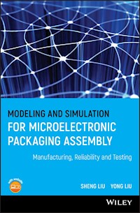
Although there is increasing need for modeling and simulation in the IC package design phase, most assembly processes and various reliability tests are still based on the time consuming "test and try out" method to obtain the best solution. Modeling and simulation can easily ensure virtual Design of Experiments (DoE) to achieve the optimal solution. This has greatly reduced the cost and production time, especially for new product development. Using modeling and simulation will become increasingly necessary for future advances in 3D package development. In this book, Liu and Liu allow people in the area to learn the basic and advanced modeling and simulation skills to help solve problems they encounter. * Models and simulates numerous processes in manufacturing, reliability and testing for the first time * Provides the skills necessary for virtual prototyping and virtual reliability qualification and testing * Demonstrates concurrent engineering and co-design approaches for advanced engineering design of microelectronic products * Covers packaging and assembly for typical ICs, optoelectronics, MEMS, 2D/3D SiP, and nano interconnects * Appendix and color images available for download from the book's companion website Liu and Liu have optimized the book for practicing engineers, researchers, and post-graduates in microelectronic packaging and interconnection design, assembly manufacturing, electronic reliability/quality, and semiconductor materials. Product managers, application engineers, sales and marketing staff, who need to explain to customers how the assembly manufacturing, reliability and testing will impact their products, will also find this book a critical resource. Appendix and color version of selected figures can be found at www.wiley.com/go/liu/packaging
Sie lesen das E-Book in den Legimi-Apps auf:
Seitenzahl: 885
Veröffentlichungsjahr: 2011
Ähnliche
Contents
Cover
Title Page
Copyright
Foreword by C. P. Wong
Foreword by Zhigang Suo
Preface
Acknowledgments
About the Authors
Part I: Mechanics and Modeling
Chapter 1: Constitutive Models and Finite Element Method
1.1 Constitutive Models for Typical Materials
1.2 Finite Element Method
1.3 Chapter Summary
References
Chapter 2: Material and Structural Testing for Small Samples
2.1 Material Testing for Solder Joints
2.2 Scale Effect of Packaging Materials
2.3 Two-Ball Joint Specimen Fatigue Testing
2.4 Chapter Summary
References
Chapter 3: Constitutive and User-Supplied Subroutines for Solders Considering Damage Evolution
3.1 Constitutive Model for Tin-Lead Solder Joint
3.2 Visco-Elastic-Plastic Properties and Constitutive Modeling of Underfills
3.3 A Damage Coupling Framework of Unified Viscoplasticity for the Fatigue of Solder Alloys
3.4 User-Supplied Subroutines for Solders Considering Damage Evolution
3.5 Chapter Summary
References
Chapter 4: Accelerated Fatigue Life Assessment Approaches for Solders in Packages
4.1 Life Prediction Methodology
4.2 Accelerated Testing Methodology
4.3 Constitutive Modeling Methodology
4.4 Solder Joint Reliability via FEA
4.5 Life Prediction of Flip-Chip Packages
4.6 Chapter Summary
References
Chapter 5: Multi-Physics and Multi-Scale Modeling
5.1 Multi-Physics Modeling
5.2 Multi-Scale Modeling
5.3 Chapter Summary
References
Chapter 6: Modeling Validation Tools
6.1 Structural Mechanics Analysis
6.2 Requirements of Experimental Methods for Structural Mechanics Analysis
6.3 Whole Field Optical Techniques
6.4 Thermal Strains Measurements Using Moiré Interferometry
6.5 In-Situ Measurements on Micro-Machined Sensors
6.6 Real-Time Measurements Using Speckle Interferometry*
6.7 Image Processing and Computer Aided Optical Techniques
6.8 Real-Time Thermal-Mechanical Loading Tools
6.9 Warpage Measurement Using PM-SM System
6.10 Chapter Summary
References
Chapter 7: Application of Fracture Mechanics
7.1 Fundamental of Fracture Mechanics
7.2 Bulk Material Cracks in Electronic Packages
7.3 Interfacial Fracture Toughness
7.4 Three-Dimensional Energy Release Rate Calculation
7.5 Chapter Summary
References
Chapter 8: Concurrent Engineering for Microelectronics
8.1 Design Optimization
8.2 New Developments and Trends in Integrated Design Tools
8.3 Chapter Summary
References
Part II: Modeling in Microelectronic Packaging and Assembly
Chapter 9: Typical IC Packaging and Assembly Processes
9.1 Wafer Process and Thinning
9.2 Die Pick Up
9.3 Die Attach
9.4 Wire Bonding
9.5 Molding
9.6 Leadframe Forming/Singulation
9.7 Chapter Summary
References
Chapter 10: Opto Packaging and Assembly
10.1 Silicon Substrate Based Opto Package Assembly
10.2 Welding of a Pump Laser Module
10.3 Chapter Summary
References
Chapter 11: MEMS and MEMS Package Assembly
11.1 A Pressure Sensor Packaging (Deformation and Stress)
11.2 Mounting of Pressure Sensor
11.3 Thermo-Fluid Based Accelerometer Packaging*
11.4 Plastic Packaging for a Capacitance Based Accelerometer*
11.5 Tire Pressure Monitoring System (TPMS) Antenna
11.6 Thermo-Fluid Based Gyroscope Packaging
11.7 Microjets for Radar and LED Cooling
11.8 Air Flow Sensor
11.9 Direct Numerical Simulation of Particle Separation by Direct Current Dielectrophoresis
11.10 Modeling of Micro-Machine for Use in Gastrointestinal Endoscopy
11.11 Chapter Summary
References
Chapter 12: System in Package (SIP) Assembly
12.1 Assembly Process of Side by Side Placed SIP
12.2 Impact of the Nonlinear Materials Behaviors on the Flip-Chip Packaging Assembly Reliability
12.3 Stacked Die Flip-Chip Assembly Layout and the Material Selection
12.4 Chapter Summary
References
Part III: Modeling in Microelectronic Package Reliability and Test
Chapter 13: Wafer Probing Test
13.1 Probe Test Model
13.2 Parameter Probe Test Modeling Results and Discussions
13.3 Comparison Modeling: Probe Test versus Wire Bonding
13.4 Design of Experiment (DOE) Study and Correlation of Probing Experiment and FEA Modeling
13.5 Chapter Summary
References
Chapter 14: Power and Thermal Cycling, Solder Joint Fatigue Life
14.1 Die Attach Process and Material Relations
14.2 Power Cycling Modeling and Discussion
14.3 Thermal Cycling Modeling and Discussion
14.4 Methodology of Solder Joint Fatigue Life Prediction
14.5 Fatigue Life Prediction of a Stack Die Flip-Chip on Silicon (FSBGA)
14.6 Effect of Cleaned and Non-Cleaned Situations on the Reliability of Flip-Chip Packages
14.7 Chapter Summary
References
Chapter 15: Passivation Crack Avoidance
15.1 Ratcheting-Induced Stable Cracking: A Synopsis
15.2 Ratcheting in Metal Films
15.3 Cracking in Passivation Films
15.4 Design Modifications
15.5 Chapter Summary
References
Chapter 16: Drop Test
16.1 Controlled Pulse Drop Test
16.2 Free Drop
16.3 Portable Electronic Devices Drop Test and Simulation
16.4 Chapter Summary
References
Chapter 17: Electromigration
17.1 Basic Migration Formulation and Algorithm
17.2 Electromigration Examples from IC Device and Package
17.3 Chapter Summary
References
Chapter 18: Popcorning in Plastic Packages
18.1 Statement of Problem
18.2 Analysis
18.3 Results and Comparisons
18.4 Chapter Summary
References
Part IV: Modern Modeling and Simulation Methodologies: Application to Nano Packaging
Chapter 19: Classical Molecular Dynamics
19.1 General Description of Molecular Dynamics Method
19.2 Mechanism of Carbon Nanotube Welding onto the Metal
19.3 Applications of Car–Parrinello Molecular Dynamics
19.4 Nano-Welding by RF Heating
19.5 Chapter Summary
References
Index
This edition first published 2011
© 2011 Chemical Industry Press. All rights reserved.
Published by JohnWiley & Sons (Asia) Pte Ltd, 1 FusionopolisWalk, #07-01 Solaris South Tower, Singapore 138628, under exclusive license by Chemical Industry Press in all media and all languages throughout the world excluding Mainland China and excluding Simplified and Traditional Chinese languages.
For details of our global editorial offices, for customer services and for information about how to apply for permission to reuse the copyright material in this book please see our website at www.wiley.com.
All Rights Reserved. No part of this publication may be reproduced, stored in a retrieval system or transmitted, in any form or by any means, electronic, mechanical, photocopying, recording, scanning, or otherwise, except as expressly permitted by law, without either the prior written permission of the Publisher, or authorization through payment of the appropriate photocopy fee to the Copyright Clearance Center. Requests for permission should be addressed to the Publisher, John Wiley & Sons (Asia) Pte Ltd, 1 Fusionopolis Walk, #07-01 Solaris South Tower, Singapore 138628, tel: 65-66438000, fax: 65-66438008, email: [email protected].
Wiley also publishes its books in a variety of electronic formats. Some content that appears in print may not be available in electronic books.
Designations used by companies to distinguish their products are often claimed as trademarks. All brand names and product names used in this book are trade names, service marks, trademarks or registered trademarks of their respective owners. The Publisher is not associated with any product or vendor mentioned in this book. This publication is designed to provide accurate and authoritative information in regard to the subject matter covered. It is sold on the understanding that the Publisher is not engaged in rendering professional services. If professional advice or other expert assistance is required, the services of a competent professional should be sought.
Library of Congress Cataloging-in-Publication Data
Liu, S. (Sheng), 1963-
Modeling and simulation for microelectronic packaging assembly: manufacturing, reliability and testing / Sheng Liu, Yong Liu.
p. cm.
Includes bibliographical references and index.
ISBN 978-0-470-82780-2 (hardback)
1. Microelectronic packaging–Simulation methods. I. Liu, Yong, 1962- II. Title.
TK7870.15.L58 2011
621.381″046–dc23
2011019534
Print ISBN: 978-0-470-82780-2
ePDF ISBN: 978-0-470-82781-9
oBook ISBN: 978-0-470-82782-6
ePub ISBN: 978-0-470-82841-0
Mobi ISBN: 978-1-118-08282-9
Foreword
By C. P. Wong
Modeling and simulation of microelectronic packaging and assembly is a multi-disciplinary activity that relies on the expertise of sequence dependant complex processes, almost all the material types, and detailed process windows; a very challenging task for both academic people and practicing engineers. Modeling and simulation has been classified in the ITRS Roadmap in the past years as being one of the cross cutting technologies that must be mastered to enable rapid progress in this first industry. The importance of modeling and simulation has been witnessed by the increasing number of design engineers in each corporation from 20% in the early 1980s to 80% in the late 2000s in terms of recruited engineers, as it is essential to design and make the product the first time right.
The most popular methodology of design and manufacturing is called Design for X (DFX, here X refers to manufacturing, assembly, testing, reliability, maintenance, environment, and even cost), which has been widely adopted by those multinational and small high tech start-up companies. The design methodology is being adjusted to meet the requirements of a full-life cycle, the so called “concept/cradle-to-grave” product responsibility, coined by Dr. Walter L. Winterbottom of Ford Science Lab.
A packaging module and related application systems, like any other electronic systems, involve a lot of manufacturing processes from film deposition, etching, chip to wafer and wafer to wafer bonding, dicing/sigulation, and extensive reliability testing for extended-life goals of many critical products such as those used for automobile electronics, avionics, portable electronics, and so on. The defects in terms of voids, cracks, delaminations, and microstructure changes, can be induced in any step and may interact and grow in subsequent steps, imposing extreme demands on the fundamental understanding of stressing and physics of failures. Currently, the testing programs have been extensive to assure reliability during product development. An iterative, build-test-fix-later process has long been used in new product development, significant concerns are being addressed as cost effective and fast time-to-market needs may not be achievable with such an approach. In the sense of high reliability, system hardware design and manufacturing and testing are costly and time consuming, and severely limit the number of design choices within the short time frame, and do not allow enough time to explore the optimal design. With the current situation of three to six months for each generation of IC chip, it is challenging to achieve truly optimal and innovative products with so many constraints in design. Design procedure must be modified and DFX must be used so as to achieve prevention with integrated consideration of manufacturing processes, testing, and operation.
Although there is still a long way to go to enable virtual manufacturing, virtual reliability and virtual testing due to the many difficulties involved, pioneering efforts have been made since the early 1990s by outstanding professionals to shorten the gap significantly, and Professor Sheng Liu and Dr. Yong Liu are two of those brave individuals. Professor Sheng Liu and Dr. Yong Liu have been promoting the new design method in the past years to help assist engineers in material selection, manufacturing yield enhancement, appropriate rapid reliability assessment, and testing when the packaging module and system are subjected to uncertainties of material selection, process windows, and various service loadings. All these issues must be addressed prior to hardware build-up and test.
A lot of processes were first time modeled and simulated by the two authors, addressing the critical importance of modeling in manufacturing, reliability, and testing. Many books about packaging have been written. Some books have been written in which mechanics has been applied to reliability issues only. This is the first book focusing on the many detailed processes in front end, back end, even probing, wire bonding, bonding, and so on. It is the first book to cover the broad aspects from manufacturing to reliability, and to testing, with many examples of their pioneering efforts. The authors describe their contributions in detail and provide guidance to those in the field and present a design approach that must ultimately replace the build-test-fix-later process if the efficiencies and potential cost benefits of the microelectronic packaging systems are to be fully realized.
C.P. Wong IEEE Fellow Member of Academy of Engineering of the USA Former Bell Labs Fellow Regents' Professor, Georgia Institute of Technology, Atlanta, GA 30332
Foreword
By Zhigang Suo
The dramatic rise of the semiconductor industry is fundamentally changing our lives. Memory devices store all human experience, or at least the part that can be digitized. Solid-state lighting saves energy. Biochips detect cancers early and at low cost. Our brains are being scanned to unravel the molecular basis of happiness and despair. The world has become a giant computer, connecting people to people, and to a multitude of devices that extend our senses. The distinction between the computer and the human may one day become a matter of choice.
The exciting future aside, the semiconductor industry is facing major challenges. As the features on chips shrink, approaching the nanoscale, the cost for chip-making equipment has been increasing. Diverse functions are being packaged, as represented by cell phones, power electronics, MEMS, solar cells, and deformable electronics. Complex manufacturing processes inevitably generate defects, which may lower the yield or result in low returns. For an industry particularly sensitive to cost and time-to-market, it has become increasingly difficult to create technologies and design products by using the trial-and-error approach.
Simulation based on mechanics has long been important for the aerospace and automobile industries, and is becoming more and more important in the semiconductor industry. The strong industrial needs have attracted many researchers to develop methods to simulate manufacturing processes and testing methods. While the dream of virtual manufacturing and virtual testing may not fully come true in the near future, simulation has already begun to reduce the amount of trial-and-error manufacturing and uncontrolled testing. The sustained effort will make the technology greener.
The authors of this book, Professor Sheng Liu and Dr. Yong Liu, are outstanding researchers and engineers. Since early 1990s, they have been intimately involved in pioneering efforts in simulating almost all the major manufacturing processes, ranging from plastic packaging to nano welding. They have devoted their careers to building material databases, developing constitutive models, finding ways to validate the models, constantly refining them, and using the models to solve practical problems. They have applied mechanics to various industry sectors, including commercial electronics, automobile electronics, powering electronics, CPUs, micro sensors, and solid-state lighting. Their experience is distilled in this book. The book is an important addition to mechanics and microelectronics, as well as to other industries that involve sophisticated manufacturing processes and testing methods.
Zhigang Suo, PhD Allen E. and Marilyn M. Puckett Professor of Mechanics and Materials School of Engineering and Applied Sciences, Kavli Institute for Bionano Science and Technology Member of the U.S. National Academy of Engineering ASME Fellow Harvard University Cambridge, Massachusetts 02138, USA
Preface
Over the past two decades semiconductor technology has made impressive progress, particularly in electronics, opto electronics, communications, health, automotive applications, computing, consumer electronics, security, and industrial electronics. These progresses are powered by Moore's law which is focusing on IC miniaturization down to nano dimensions and system on chip (SoC) integration. However, there are technologies based on or derived from silicon technologies but which do not simply scale with Moore's law such as the RF, power electronics, sensors, MEMS, opto/lighting and other systems in package; these technologies are called “More than Moore”. Along with the technology development trends characterized by Moore's law and “More than Moore”, the business trends are mainly characterized by cost reduction, shortertime-to-market, and outsourcing. The combination of these technology and business trends leads to increased design complexity, decreased design margins, increased chances and consequences of failure in reliability, decreased product development in R&D, and difficulties in assembly manufacture and qualification times. Especially in the assembly manufacturing process, quality and reliability are key technologies to ensure a successful product. In addition to the forward looking trends of technology it is important to recognize that the methods for concurrent engineering of these solutions (both the semiconductor content and high performance package capability) are becoming increasingly dependent on rigorous use of proven multi-physics/finite element analysis (FEA) tools and techniques for both new product development and its assembly processes. The correct use of the modeling tool can definitely save design time and shorten the design cycle. The challenges are along with the development of new package technology; can the modeling tools and methodologies be ready to support the new trends? Examples are various designs, reliability and assembly manufacture modeling which include electro migration simulation; diffusion along the interface of two metal materials; contamination at the interface between leadframe, multiple chips and EMC; thermal resistance definition in system in package (SiP); 3D copper stud bumping, wire bonding simulation, and so on.
Most challenges in modeling for electronic packaging today are the fundamental multiple-physics simulation which couples the electrical, thermal, and mechanical fields for various assembly manufacturing processes and for various reliability tests. Development of a highly efficient modeling algorithm for such a SiP system is critical for the virtual prototyping of the new product. In some cases, the SiP might have strong thermal mechanical performance but is weak in the electrical area, or the SiP has very good electrical performance but is weak in thermal-mechanical design. Therefore, it is necessary to establish the best solution using the modeling design of experiment (DoE) while the actual tests or actual assembly manufacturing will cost more and take much longer.
In industry, we all understand the importance of assembly manufacturing, reliability, and testing, because a lot of packaging failures are related to the assembly process. Examples include the wire bonding process, which would induce silicon cratering, bond pad peel off, and interlayer dielectric (ILD) layer under bond pad cracking; die attaching process for multiple die; the order of the die attaching process will have a big impact on the residual stress after the die bonding. When thin die (today the thinnest die thickness would be below 20 microns) is picked up from the tape, the pick-up process could crack the silicon. The molding process is also a key process which could induce later failure, such as delamination due to the voids tracked in the interface between the leadframe and encapsulate molding compound (EMC). Leadframe forming, punch/simulation, and trim may result in the die and package cracking as well. A lot of initial tiny defects are induced in first assembly manufacture process; later in the further assembly process and reliability test, they become potential product quality and reliability concerns. An example is wafer sorting, which will induce the cratering/marks on the bond pad. When the wire bonding process is applied to the cratered/marked bond pad, it will definitely impact the adhesion strength at the interface between the wire bond and the bond pad. Product line engineers are always interested in knowing wire bonding versus wafer probing; which makes things worse? The study of assembly manufacture processes through modeling and simulation started from the beginning of the IC packaging, and today the need for modeling and simulation in this area has increased much more. However, at the present time, there is no book that has systematically described the modeling methodologies for assembly manufacturing, reliability, and testing, as well as discussing the above challenges and giving the readers some unresolved space for further exploring. This is our goal in writing this book; to share our modeling experiences and systematically introduce our modeling methodologies for electronic packaging assembly manufacturing, reliability and testing.
This book is primarily concerned with studies of electronic packaging in assembly manufacture processes and failure mechanisms in assembly manufacture processes and tests through modeling and simulation. However, the fundamental studies regarding the advanced modeling methodologies including molecular dynamics, state of the art simulation algorithms, material constitutive relations, material behavior testing, and various semiconductor reliability tests are also discussed and presented in the book. Various package layouts including the 3D/TSV/Stacking/SiP, carbon nano-tube and interconnects technology, opto packaging, and MEMS are discussed and presented in the book as well. A lot of case studies provide the most advanced research progress and the topics that industry is interested in. The basic framework of this book is arranged in four parts, the first part (Part I) includes eight chapters that introduce the fundamental mechanics concepts, material constitutive models, basic modeling methodologies such as finite element, and the concurrent engineering background for microelectronics. This part is to provide readers with the background knowledge for modeling and simulation, mechanics, material, and the engineering. The next part (Part II) is concerned with the modeling in microelectronic packaging and the assembly manufacturing process which includes five chapters. Major topics include the electronic packaging front of line (which involves key processes such as wafer sorting, die picking up, die attach process, wire bonding); end of line (which includes molding, leadframe clamping, forming, and singulation); Opto packaging assembly; MEMS packaging assembly; system in packaging stack/3D assembly and the Nano interconnects and packaging assembly. Part III describes the modeling in reliability and testing which includes the wafer probing test and typical package reliability tests such as the temperature cycle test, power cycle test, drop test, electro-migration test, precondition test with reflow which includes moisture sensitivity test, vapor pressure at reflow with the popcorning failure mechanisms. The advanced simulation algorithm will be presented especially in the wafer level CSP solder joint reliability in drop test, temperature cycling, and the mass migration induced failure which includes electro migration, thermal migration, stress migration, and the atomic density gradient induced migration. The final part will introduce the modern modeling and simulation methodologies which include the classical molecular dynamics, advanced molecular dynamics, and coupling with continuum modeling methods. This part will disclose how the modern modeling and simulation methodologies will impact the assembly manufacturing, reliability and the testing for today and future advanced package development. An appendix is available on the book companion web site for those who like to know more detail about finite element.
Sheng Liu, Ph.D., ASME Fellow ChangJiang Scholar Professor School of Mechanical Science and Engineering and Wuhan National Laboratory for Optoelectronics Huazhong University of Science and Technology Wuhan, Hubei, China
Yong Liu, PhD, IEEE Senior Member Senior Member of Technical Staff Fairchild Semiconductor Corporation South Portland, Maine, USA
Acknowledgments
Development and preparation of Modeling and Simulation for Microelectronic Packaging Assembly: Manufacturing, Reliability and Testing was facilitated by a number of dedicated people at John Wiley & Sons, Chemical Industry Press, and Huazhong University of Science and Technology. We would like to thank all of them, with special mentions for Gang Wu of Chemical Industry Press, James W. Murphy of John Wiley & Sons, and Bin Song, the research assistant of the first author, at Huazhong University of Science and Technology. Without them, our dream of this book would not have come true, as they have worked so hard on the preparation of the book. It has been a great pleasure and fruitful experience to work with them in transferring our manuscript into a very attractive printed book.
The materials in this book have clearly been derived mainly from previous papers and research notes by the two authors and some works of their friends which are mainly from both the research community and industry, such as Dr. Gary Li of Freescale, Dr. Yifan Guo of Skyworks, and Professor Zhigang Suo from Harvard University. It would be quite impossible for us to express our appreciation to everyone concerned for their collaboration in the production of this book, but we would like to extend our gratitude. In particular, we would like to thank several professional societies in which we have previously published some of our materials included in this book. They are the American Society of American Engineers (ASME) and the Institute of Electrical and Electronic Engineers (IEEE) for their conferences, proceedings, and journals, including ASME Transactions on Journal of Electronic Packaging, IEEE Transactions on Advanced Packaging, IEEE Transactions on Components and Packaging Technology and IEEE Transactions on Electronics Packaging Manufacturing. Many important conferences such as the Electronic Components and Technology Conference (ECTC), and International Conference on Electronic Packaging Technology and High Density Packaging (ICEPT–HDP), EuroSime are also appreciated for the reproduction of some of their publication materials.
We would like to acknowledge those colleagues who helped review some chapters and manuscript. They are Dr. YiHsin Pao of Foxcom, Professor Biao Wang of SunYiSan University, Professor Kikuo Kishimoto at Tokyo Institute of Technology, and Professor Ricky Lee at Hong Kong University of Science and Technology. We would like to thank them for their many suggestions and comments which added a lot to this book. Their depth of knowledge and their dedication have been demonstrated throughout the process of reviewing this book and its chapters.
We would like to thank Huazhong University of Science and Technology (HUST), Wuhan National Laboratory for Optoelectronics, the School of Mechanical Science and Engineering, and Fairchild Semiconductor Corporation for providing us with excellent working environment to make this book possible. We also appreciate those places where we have previously studied and worked, such as Stanford University, Florida Institute of Technology, and Wayne State University, where we conducted quite a significant part of our research results in the book. We would like to express our appreciation to those who have worked in microelectronic packaging and assembly for many years, such as those SRC mentors in the first author's research. The first author felt honored to have worked with Dr. William Chen and Dr. T.Y. Wu at ASE (formerly at IBM), Dr. YiFan Guo at Skyworks (formerly at IBM and Freescale), Dr. J. Benson at Harris, Dr. T.D. Dudderar at Bell Labs, Dr. L. Li at Cisco (formerly at IBM), Dr. M.J. Lii at Intel, Dr. Z. Mei at HP, Dr. S. Sidharth at AMD, Dr. L. Stark at TI, and Dr. J. Xie (forming at Moforola), Dr. S. Wu at Motorola, and Dr. Luu T. Nguyen at National.
We would like to show our thanks to our outstanding students, visiting scientists and colleagues. For the research with the first author in the USA and in China, they include Dr. Yuhai Mei, Dr. Jiansen Zhu, Dr. Jianjun Wang, Dr. Zhengfang Qian, Dr. Daqing Zou, Dr. Wei Ren, Mr. Jian Yang, Ms. Changrong Ji, Dr. Xiaohui Song, Mr. Zhaohui Chen, Professor Fulong Dai at Tsinghua University, Professor Xiaoyuan He at Southeast University, Professor Mingfu Lu, Professor Yuwen Qin at Tianjin University, Professor Wei Yang at Zhejiang University (formerly at Tsinghua University), Professors Yilong Bai, Haiying Wang, and Yapu Zhao at the Institute of Mechanics of Chinese Academy of Sciences, and Dr. Jimmy Hu at Microsoft (formerly at FOKD). For the research with the second author in the USA and China, they include Dr.Timwah Luk, Mr. Scott Irving, Mr. Richard Qian and Dr. Yumin Liu at Fairchild, Dr. Lihua Liang and Ms Shinan Wang at Fairchild–ZJUT Joint Lab, Zhejiang University of Technology.
We would like to express our appreciation to the Chinese Electronics Society and its Electronic Manufacturing and Packaging Branch led by Professor Keyun Bi for providing us with many technical and academic exchange opportunities. We particularly appreciate the excellent platform initiated jointly by us in early 1990s, the International Conference on Electronic Packaging Technology (ICEPT, now ICEPT–HDP), now an important IEEE CPMT conference in the world. We are very happy to have worked with outstanding fellows such as Professor C. P. Wong, Professor Ricky Lee, Professor Y. C. Lee, Professor Shangtong Gao, Professor JuShen Ma, Professor Shouwen Yu, Professor Xiangfu Zong, Professor Ming Li, Professor Qingchun Wang, Professor Johan Liu, Professor Xiaoyuan He, Professor Lixi Wan, Dr. Tom Chang, Dr. Daniel Shi, Dr. Guoqi Zhang, Dr. Dongkai Shanguang, Professor Mike Pecht, Professor Kuoning Chuang, Professor Xuejun Fan, Professor James Morris, and many others. Working and socializing with them has been a privilege and a pleasant experience.
We would also like to acknowledge the support of many funding agencies in the past many years such as the USA National Science Foundation, the USA SRC (Semiconductor Research Corporation), the National Natural Science Foundation of China, the Ministry of Science and Technology of China, the National S&T Major Project, the Hubei Department of Science and Technology, the Wuhan Science and Technology Bureau, the Guangdong Department of Science and Technology, the Foshan Bureau of Science and Technology, and the Nanhai Bureau of Science and Technology.
Lastly the first author would like to thank his parents, Mr. Jixian Liu and Ms. Yanrong Shen, his wife, Bin Chen, and his daughter Amy Liu, his son Aaron Liu, and the second author would like to thank both his parents and parents-in-law, his wife, Jane Chen, and his great sons Junyang Liu and Alexander Liu for their love, consideration, and patience in allowing them to work on many weekends and late nights for this book. The author's simple belief is that the contribution of this book to the LED lighting and packaging industry is worthwhile, in this rapid development of solid state lighting, and will continue to be worthwhile to our civilization for many years to come. The authors would like to dedicate this book to their families.
Sheng Liu, PhD ASME Fellow ChangJiang Scholar Professor School of Mechanical Science and Engineering and Wuhan National Laboratory for Optoelectronics Huazhong University of Science and Technology Wuhan, Hubei, China Yong Liu, PhD, IEEE Senior Member Fairchild Semiconductors Corporation South Portland, USA
About the Authors
Sheng Liu is a Changjiang scholar Professor of Mechanical Engineering at Huazhong University of Science and Technology and he has a dual appointment at Wuhan National Laboratory for Optoelectronics. He was once a tenured faculty at Wayne State University. He has over 18 years experience in LED/MEMS/IC packaging. He has extensive experience in consulting with many leading multinational and Chinese companies. He won the prestigious White House/NSF Presidential Faculty Fellow Award in 1995, the ASME Young Engineer Award in 1996, the NSFC Overseas Young Scientist Award in 1999 in China, the IEEE CPMT Exceptional Technical Achievement Award in 2009, and the Chinese Electronic Manufacturing and Packaging Technology Society Special Achievement Award in 2009. He has been an associate editor of IEEE Transactions on Electronic Packaging Manufacturing since 1999 and an associate editor of Frontiers of Optoelectronics in China since 2007. Since 2006, he has been one of the 11 National Committee Members in LED at the Ministry of Science and Technology of China. He obtained his PhD from Stanford University in 1992, his MS and BS degrees from Nanjing University of Aeronautics and Astronautics in 1986 and 1983 respectively. He was an aircraft designer at the Chengdu Aircraft Company for two years. He is also currently an ASME Fellow. He has filed and owned more than 140 patents in China and in the USA, has published more than 500 technical articles, given more than 100 keynotes and invited talks, and edited more than nine proceedings in English for the ASME and IEEE.
Yong Liu has been with Fairchild Semiconductor Corporation in South Portland, Maine since 2001; as a Senior Member of the Technical Staff from 2008, a Member of the Technical Staff from 2004–2007, and a Principal Engineer from 2001–2004. He is now a Fairchild global team leader of electrical, thermal-mechanical modeling and analysis. His main area of interest is advanced IC packaging, modeling and simulation, reliability and assembly process. In the last few years he and his team have been working on advanced IC package modeling and simulation, which includes pioneering work on the assembly manufacture process, the electromigration induced failures for chip scale wafer level packages, and co-design automation. He has been invited to give keynotes talks and presentations at international conferences such as Eurosime, ICEPT–HDP, and EPTC and at universities in the USA, Europe, and China. He has co-authored over 140 papers in journals and conferences and has filed over 40 USA patents in the area of 3D/Stack/TSV IC packaging and power devices. Dr. Liu obtained his BS, Masters, and PhD degrees at the Nanjing Univeristy of Science and Technology in 1983, 1987, and 1990 respectively. He was once promoted, in a ground-breaking way, as a full professor at Zhejiang University of Technology in 1994. Dr. Liu was awarded an Alexander von Humboldt Fellowship and studied as a Humboldt fellow at Tech University of Braunschweig, Germany in 1995. In 1997, he was awarded an Alexander von Humboldt European Fellowship and studied as a Humboldt European fellow at the University of Cambridge, England. In 1998, he worked as a post-doctor at Semiconductor Focus Center and Computational Mechanics Center, Rensselaer Polytechnic Institute (RPI). In 2000, he worked as a staff opto package engineer at Nortel Networks in Boston. Since he joined Fairchild in 2001, he was awarded the first Fairchild President Award in 2008, the Fairchild Key Technologist in 2006 and 2009, the Fairchild BIQ award in product innovation in 2005, and the Fairchild award for Power of the Pen first place in 2004. Yong Liu is currently an IEEE Senior member and has been actively involved in technical committees of the IEEE ECTC, EuroSime, ESREF, ESTC, EPTC, and ICEPT.
Part I
Mechanics and Modeling
Microelectronic devices, optoelectronic devices, and MEMS (micro-electrical-mechanical- systems) devices and their systems are mainly being manufactured with a silicon chip, or chips, in various compact package configurations to satisfy cost and performance requirements. A typical package and assembly is manufactured through many processes (both front-end and back-end), followed by many severe reliability qualification tests. A typical packaging assembly consists of components of different materials with different mechanical and thermal properties, and geometric discontinuities exist in terms of vias, comers, free edges, interfaces, surfaces, and composites. Non-uniform temperature and moisture fields during each process of packaging and assembly, testing, storage, and operation often subject these materials and components to various failure modes, for example, metal line voiding, passivation cracking, die cracking, fine metal line smearing, package swelling, warpage, and delamination. If failure occurs in a process step of manufacturing, and results in the component not being processed, yield can be a big issue, and popcorning during the reflow of plastic packaging onto the board is such an example. System functionality tests performed on these packages and assemblies, in general, will not detect the majority of these failures. This may not cause catastrophic failure but may cause performance degradation and failure before the designed life cycle. Due to the rapid advancement of the related industries, information on detailed failure initiation, growth and performance degradation is not easily available and it is a challenging task for the modeling and simulation community. Closed-form solutions are mostly unavailable due to the many nonlinearities such as material nonlinearities for many polymer and solder materials, geometrical nonlinearity such as membrane deformation in sensors, force nonlinearity such as contact and debonding, contour change for sequential process steps, micro-structural changes such as for annealing, damage development, and mass transport for electromigration and wetting, just to list a very few examples. Serious study is essential for modeling and simulation. Constitutive models for engineering materials are a must to avoid a wrong analysis which can easily result in engineers arriving at wrong conclusions or no conclusions at all. In the first part of the book, we will introduce constitutive models and leave the definition of the basic concepts such as stress, strain, and so on, to Appendix A. Then we will briefly present the finite element methods and some of the advanced features such as sub-modeling, sub-structure, and element birth and death. Material testing for small samples is presented to show the uniqueness of our samples as compared to bulk structures for traditional industries. User-supplied subroutines are also presented with solders as an example. Multi-physics and multi-scale modeling is presented by briefly introducing molecular dynamics (MD), while leaving most of MD to Part IV. Validation tools and their applications for both on-line testing and off-line quality analysis are presented. Fracture mechanics with the focus on the interfacial fracture mechanics is presented and the concurrent engineering approach is presented as a platform for leading research laboratories which are product oriented and have a strong desire to shorten the time-to-market and time-to-profit.
Chapter 1
Constitutive Models and Finite Element Method
In this chapter, the basic equations of continuum mechanics are introduced. It is assumed that the readers already have a basic prior knowledge of the subject. Therefore, lengthy derivations are omitted, such information being provided in the Appendix. Only equations that are needed later for deriving the mechanics theories are outlined. Most equations are adopted from several famous references listed in the literature of this chapter, including ABAQUS theory manual (Belytschko et al., 2000; Hibbit et al., 2008).
1.1 Constitutive Models for Typical Materials
1.1.1 Linear Elasticity
In many engineering applications involving small strains and rotations, the response of the material may be considered to be linearly elastic. The most general way to represent elastic tensor C relation between the stress and strain tensors is given by:
(1.1)
where Cijkl are components of the 4th-order tensor of elastic moduli. This equation is the generalized Hooke's law which incorporates a fully anisotropic material response.
The strain energy per unit volume, often called the elastic potential, W, is generalized to multiaxial states by:
(1.2)
The stress is then given by:
(1.3)
which is the tensor equivalent of Equation (1.2). The strain energy is assumed to be positive definite:
(1.4)
with equality if and only if which implies that C is a positive-definite 4th-order tensor. From the symmetries of the stress and strain tensors, the material coefficients have the so called minor symmetries:
(1.5)
and from the existence of a strain energy potential Equation (1.2) it follows that:
(1.6)
If W is a smooth function of ε, Equation (1.6) implies a property called major symmetry:
(1.7)
since smoothness implies:
(1.8)
The general 4th-order tensor Cijkl has independent constants. These 81 constants may also be interpreted as arising from the necessity to relate nine components of the complete stress tensor to nine components of the complete strain tensor, that is, 9 × 9 = 81. The symmetries of the stress and strain tensors require only that six independent components of stress be related to six independent components of strain. The resulting minor symmetries of the elastic moduli therefore reduce the number of independent constants to 6 × 6 = 36. Major symmetry of the moduli, expressed through Equation (1.7) reduces the number of independent elastic constants to , for n = 6, that is, the number of independent components of a 6 × 6 matrix.
Considerations of material symmetry further reduce the number of independent material constants. An isotropic material is one which has no preferred orientations or directions in its properties, so that the stress-strain relation is identical when expressed in component form in any rectangular Cartesian coordinate system. The most general constant isotropic 4th-order tensor can be shown to be a linear combination of terms comprised of Kronecker deltas, that is, for an isotropic linearly elastic material:
Lesen Sie weiter in der vollständigen Ausgabe!
Lesen Sie weiter in der vollständigen Ausgabe!
Lesen Sie weiter in der vollständigen Ausgabe!
Lesen Sie weiter in der vollständigen Ausgabe!
Lesen Sie weiter in der vollständigen Ausgabe!
Lesen Sie weiter in der vollständigen Ausgabe!
Lesen Sie weiter in der vollständigen Ausgabe!
Lesen Sie weiter in der vollständigen Ausgabe!
Lesen Sie weiter in der vollständigen Ausgabe!
Lesen Sie weiter in der vollständigen Ausgabe!
Lesen Sie weiter in der vollständigen Ausgabe!
Lesen Sie weiter in der vollständigen Ausgabe!
Lesen Sie weiter in der vollständigen Ausgabe!
Lesen Sie weiter in der vollständigen Ausgabe!
Lesen Sie weiter in der vollständigen Ausgabe!
Lesen Sie weiter in der vollständigen Ausgabe!
Lesen Sie weiter in der vollständigen Ausgabe!
Lesen Sie weiter in der vollständigen Ausgabe!
Lesen Sie weiter in der vollständigen Ausgabe!
Lesen Sie weiter in der vollständigen Ausgabe!
Lesen Sie weiter in der vollständigen Ausgabe!
Lesen Sie weiter in der vollständigen Ausgabe!
