109,99 €
Mehr erfahren.
- Herausgeber: John Wiley & Sons
- Kategorie: Fachliteratur
- Serie: A Wiley-Science Wise Co-Publication
- Sprache: Englisch
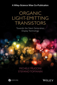
Provides an overview of the developments and applications of Organic Light Emitting Transistors (OLETs) science and technology
This book discusses the scientific fundamentals and key technological features of Organic Light Emitting Transistors (OLETs) by putting them in the context of organic electronics and photonics. The characteristics of OLETs are benchmarked to those of OLEDs for applications in Flat Panel Displays and sensing technology. The authors provide a comparative analysis between OLED and OLET devices in order to highlight the fundamental differences in terms of device architecture and working principles, and to point out the enabling nature of OLETs for truly flexible displays. The book then explores the principles of OLET devices, their basic optoelectronic characteristics, the properties of currently available materials, processing and fabrication techniques, and the different approaches adopted to structure the active channel and to control organic and hybrid interfaces.
- Examines the photonic properties of OLETs, focusing on the external quantum efficiency, the brightness, the light outcoupling, and emission directionality
- Analyzes the charge transport and photophysical properties of OLET, emphasizing the excitonic properties and spatial emitting characteristics
- Reviews the key building blocks of the OLET devices and their role in determining the device’s performance
- Discusses the challenges in OLET design, namely color gamut, power efficiency, and reliability
- Presents key applications of OLET devices and their potential impact on display technology and sensing
Sie lesen das E-Book in den Legimi-Apps auf:
Seitenzahl: 504
Veröffentlichungsjahr: 2016
Ähnliche
Table of Contents
COVER
TITLE PAGE
1 INTRODUCTION
2 ORGANIC LIGHT-EMITTING DIODES
2.1 OLED DEVICE STRUCTURE AND WORKING PRINCIPLES
2.2 APPLICATIONS OF OLED TECHNOLOGY
2.3 DIODE VERSUS TRANSISTOR ARCHITECTURE FOR LIGHT EMISSION
2.4 CONCLUSIONS
REFERENCES
3 ORGANIC LIGHT-EMITTING TRANSISTORS
3.1 WORKING PRINCIPLES OF OLETs
3.2 DEVICE STRUCTURES
3.3 THIN-FILM OLETs
3.4 SINGLE-CRYSTAL OLET
3.5 CONCLUSIONS
REFERENCES
4 KEY BUILDING BLOCKS OF OLETs
4.1 DIELECTRIC LAYER
4.2 EMISSIVE AMBIPOLAR SEMICONDUCTORS
4.3 CHARGE-INJECTING ELECTRODES
4.4 CONCLUSIONS
REFERENCES
5 CHARGE-TRANSPORT AND PHOTOPHYSICAL PROCESSES IN OLETs
5.1 CHARGE TRANSPORT IN OLETs
5.2 FUNDAMENTAL EXCITONIC PROCESSES AND MODELING OF OLETs
5.3 EXCITONIC RECOMBINATION AND EMITTING AREA IN OLETs
5.4 CONCLUSIONS
REFERENCES
6 PHOTONIC PROPERTIES OF OLETs
6.1 EXTERNAL QUANTUM EFFICIENCY
6.2 BRIGHTNESS
6.3 LIGHT OUTCOUPLING AND EMISSION DIRECTIONALITY
6.4 A POSSIBLE ROUTE FOR ORGANIC INJECTION LASING
6.5 CONCLUSIONS
REFERENCES
7 APPLICATIONS OF ORGANIC LIGHT-EMITTING TRANSISTORS
7.1 OLET DISPLAY TECHNOLOGY
7.2 OLET-BASED SENSING
7.3 OPEN ISSUES AND NEXT DEVELOPMENT TARGETS
7.4 CONCLUSIONS
REFERENCES
8 CONCLUSIONS
INDEX
END USER LICENSE AGREEMENT
List of Tables
Chapter 04
Table 4.1 (a) Electron and Hole Field-Effect Mobility (
μ
) Data as a Function of the SiO
2
Surface Treatment, Gate Threshold (
V
t
) Values for Electron and Hole Transport, and the Δ
V
t
Hysteresis Values.
Chapter 06
Table 6.1 Summary of the Emission Characteristics and Performance Figures of the Ambipolar F8BT OLETs with Different PMMA Thicknesses.
List of Illustrations
Chapter 02
Figure 2.1 Multilayer OLED device structure (a) and working principle (b).
Figure 2.2 (a, b) Electronic processes of host–guest molecules, in which the guest molecules can emit light through both singlet and triplet states. , : a singlet ground state of the host and guest molecules, respectively. , : a first excited singlet state of the host and guest molecules, respectively. , : a first excited triplet state of the host and guest molecules, respectively.
Figure 2.3 Comparison between the (simplified) energy level diagram for standard phosphorescent (a) and TADF-based (b) emitters. Important rates
ki
are indicated.
r
, radiative;
nr
, nonradiative;
F
, fluorescence;
P
, phosphorescence; ISC, intersystem crossing; RISC, reverse ISC; Δ
E
ST
, singlet–triplet splitting.
Figure 2.4 (a) Cross section of an OLED with indication of different light modes. (b) Typical power spectrum of the internally generated light shown as a function of the in-plane wavevector. Vertical lines separate the various possible light modes. Neither waveguide (wg) nor evanescent modes (thick line) can be accessed with external-light outcoupling techniques; thus, they dissipate within the layer structure. Model calculation [36] for a bottom-emitting device similar to devices discussed in Reference [37].
Figure 2.5 (a) Schematic of the OLED device structure on low-cost flexible plastic with metal electrodes. (b) Photograph of a large-area flexible OLED (50 × 50 mm
2
) working at high luminance (>5000 cd/m
2
).
Figure 2.6 Energy level diagram in an OLED reported in Reference 47. Lines correspond to HOMO (solid) and LUMO (dashed) energies; filled boxes refer to the triplet energies. The orange color marks intrinsic regions of the emission layer. F and D represent Förster- and Dexter-type energy exchange channels, respectively. The orange dashed box depicts the main region of exciton generation.
Figure 2.7 Current status of energy conversion efficiency of OLEDs (in solid circles) and LEDs (in open rhombuses) in the visible spectrum. The LED data were taken from [64]. The OLED efficiencies are power efficiencies of the device at 1000 cd/m
2
after applying the outcoupling enhancement technique listed in Reference 48 and normalized to the theoretical limit for the corresponding wavelength. The OLED data were taken from References [37,48,57,65–70]. The dashed gray curve represents the photopic sensitivity response curve of the human eyes.
Lesen Sie weiter in der vollständigen Ausgabe!
Lesen Sie weiter in der vollständigen Ausgabe!
Lesen Sie weiter in der vollständigen Ausgabe!
Lesen Sie weiter in der vollständigen Ausgabe!
Lesen Sie weiter in der vollständigen Ausgabe!
Lesen Sie weiter in der vollständigen Ausgabe!
Lesen Sie weiter in der vollständigen Ausgabe!
Lesen Sie weiter in der vollständigen Ausgabe!
Lesen Sie weiter in der vollständigen Ausgabe!
Lesen Sie weiter in der vollständigen Ausgabe!
Lesen Sie weiter in der vollständigen Ausgabe!
Lesen Sie weiter in der vollständigen Ausgabe!


