70,99 €
Mehr erfahren.
- Herausgeber: John Wiley & Sons
- Kategorie: Fachliteratur
- Sprache: Englisch
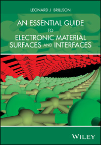
An Essential Guide to Electronic Material Surfaces and Interfaces is a streamlined yet comprehensive introduction that covers the basic physical properties of electronic materials, the experimental techniques used to measure them, and the theoretical methods used to understand, predict, and design them.
Starting with the fundamental electronic properties of semiconductors and electrical measurements of semiconductor interfaces, this text introduces students to the importance of characterizing and controlling macroscopic electrical properties by atomic-scale techniques. The chapters that follow present the full range of surface and interface techniques now being used to characterize electronic, optical, chemical, and structural properties of electronic materials, including semiconductors, insulators, nanostructures, and organics. The essential physics and chemistry underlying each technique is described in sufficient depth for students to master the fundamental principles, with numerous examples to illustrate the strengths and limitations for specific applications. As well as references to the most authoritative sources for broader discussions, the text includes internet links to additional examples, mathematical derivations, tables, and literature references for the advanced student, as well as professionals in these fields. This textbook fills a gap in the existing literature for an entry-level course that provides the physical properties, experimental techniques, and theoretical methods essential for students and professionals to understand and participate in solid-state electronics, physics, and materials science research.
An Essential Guide to Electronic Material Surfaces and Interfaces is an introductory-to-intermediate level textbook suitable for students of physics, electrical engineering, materials science, and other disciplines. It is essential reading for any student or professional engaged in surface and interface research, semiconductor processing, or electronic device design.
Sie lesen das E-Book in den Legimi-Apps auf:
Seitenzahl: 541
Veröffentlichungsjahr: 2016
Ähnliche
Table of Contents
Cover
Title Page
Copyright
Preface
About the Companion Websites
Chapter 1: Why Surfaces and Interfaces of Electronic Materials
1.1 The Impact of Electronic Materials
1.2 Surface and Interface Importance as Electronics Shrink
1.3 Historical Background
1.4 Next Generation Electronics
1.5 Problems
References
Further Reading
Chapter 2: Semiconductor Electronic and Optical Properties
2.1 The Semiconductor Band Gap
2.2 The Fermi Level and Energy Band Parameters
2.3 Band Bending at Semiconductor Surfaces and Interfaces
2.4 Surfaces and Interfaces in Electronic Devices
2.5 Effects of Localized States: Traps, Dipoles, and Barriers
2.6 Summary
2.7 Problems
References
Further Reading
Chapter 3: Electrical Measurements of Surfaces and Interfaces
3.1 Sheet Resistance and Contact Resistivity
3.2 Contact Measurements: Schottky Barrier Overview
3.3 Heterojunction Band Offsets: Electrical Measurements
3.4 Summary
3.5 Problems
References
Further Reading
Chapter 4: Localized States at Surfaces and Interfaces
4.1 Interface State Models
4.2 Intrinsic Surface States
4.3 Extrinsic Surface States
4.4 The Solid State Interface: Changing Perspectives
4.5 Problems
References
Further Reading
Chapter 5: Ultrahigh Vacuum Technology
5.1 Ultrahigh Vacuum Chambers
5.2 Pumps
5.3 Manipulators
5.4 Gauges
5.5 Residual Gas Analysis
5.6 Deposition Sources
5.7 Deposition Monitors
5.8 Summary
5.9 Problems
References
Further Reading
Chapter 6: Surface and Interface Analysis
6.1 Surface and Interface Techniques
6.2 Excited Electron Spectroscopies
6.3 Principles of Surface Sensitivity
6.4 Multi-technique UHV Chambers
6.5 Summary
6.6 Problems
References
Further Reading
Chapter 7: Surface and Interface Spectroscopies
7.1 Photoemission Spectroscopy
7.2 Auger Electron Spectroscopy
7.3 Electron Energy Loss Spectroscopy
7.4 Rutherford Backscattering Spectrometry
7.5 Surface and Interface Technique Summary
7.6 Problems
References
Further Reading
Chapter 8: Dynamical Depth-Dependent Analysis and Imaging
8.1 Ion Beam-Induced Surface Ablation
8.2 Auger Electron Spectroscopy
8.3 X-Ray Photoemission Spectroscopy
8.4 Secondary Ion Mass Spectrometry
8.5 Spectroscopic Imaging
8.6 Depth-Resolved and Imaging Summary
8.7 Problems
References
Further Reading
Chapter 9: Electron Beam Diffraction and Microscopy of Atomic-Scale Geometrical Structure
9.1 Low Energy Electron Diffraction – Principles
9.2 Reflection High Energy Electron Diffraction
9.3 Scanning Electron Microscopy
9.4 Transmission Electron Microscopy
9.5 Electron Beam Diffraction and Microscopy Summary
9.6 Problems
References
Further Reading
Chapter 10: Scanning Probe Techniques
10.1 Atomic Force Microscopy
10.2 Scanning Tunneling Microscopy
10.3 Ballistic Electron Energy Microscopy
10.4 Atomic Positioning
10.5 Summary
10.6 Problems
References
Further Reading
Chapter 11: Optical Spectroscopies
11.1 Overview
11.2 Optical Absorption
11.3 Modulation Techniques
11.4 Multiple Surface Interaction Techniques
11.5 Spectroscopic Ellipsometry
11.6 Surface Enhanced Raman Spectroscopy
11.7 Surface Photoconductivity
11.8 Surface Photovoltage Spectroscopy
11.9 Photoluminescence Spectroscopy
11.10 Cathodoluminescence Spectroscopy
11.11 Summary
11.12 Problems
References
Further Reading
Chapter 12: Electronic Material Surfaces
12.1 Geometric Structure
12.2 Chemical Structure
12.3 Electronic Structure
12.4 Summary
12.5 Problems
References
Further Reading
Chapter 13: Surface Electronic Applications
13.1 Charge Transfer and Band Bending
13.2 Oxide Gas Sensors
13.3 Granular Gas Sensors
13.4 Nanowire Sensors
13.5 Chemical and Biosensors
13.6 Surface Electronic Temperature, Pressure, and Mass Sensors
13.7 Summary
13.8 Problems
References
Further Reading
Chapter 14: Semiconductor Heterojunctions
14.1 Geometrical Structure
14.2 Chemical Structure
14.3 Electronic Structure
14.4 Conclusions
14.5 Problems
References
Further Reading
Chapter 15: Metal–Semiconductor Interfaces
15.1 Overview
15.2 Metal–Semiconductor Interface Dipoles
15.3 Interface States
15.4 Self-Consistent Electrostatic Calculations
15.5 Experimental Schottky Barriers
15.6 Interface Barrier Height Engineering
15.7 Atomic-Scale Control
15.8 Summary
15.9 Problems
References
Further Reading
Chapter 16: Next Generation Surfaces and Interfaces
16.1 Current Status
16.2 Current Device Challenges
16.3 Emerging Directions
16.4 The Essential Guide Conclusions
Appendix A: Glossary of Commonly Used Symbols
Appendix B: Table of Acronyms
Appendix C: Table of Physical Constants and Conversion Factors
Appendix D: Semiconductor Properties
Index
End User License Agreement
Pages
xiii
xv
1
2
3
4
5
6
7
8
9
10
11
12
13
14
15
16
17
18
19
20
21
22
23
24
25
26
27
28
29
30
31
32
33
34
35
36
37
38
39
40
41
42
43
44
45
46
47
48
49
50
51
52
53
54
55
56
57
58
59
60
61
62
63
64
65
66
67
68
69
70
71
72
73
74
75
76
76
77
77
78
78
79
79
80
80
81
82
81
82
83
83
84
84
85
86
87
88
89
90
91
92
93
94
95
96
97
98
99
100
101
102
103
104
105
106
107
108
109
110
111
112
113
114
115
116
117
118
119
120
121
122
123
124
125
126
127
128
129
130
131
132
133
134
135
136
137
138
139
140
141
142
143
144
145
146
147
148
149
150
152
153
154
155
156
157
158
159
160
161
162
163
164
165
166
167
168
169
170
171
172
173
174
175
176
177
178
179
180
181
182
183
184
185
186
187
188
189
190
191
192
193
194
195
196
197
198
199
200
201
202
203
204
205
206
207
208
209
210
211
212
213
214
215
216
217
218
219
220
221
222
223
224
225
226
227
228
229
230
231
232
233
234
235
236
237
238
239
240
241
242
243
244
245
246
247
248
249
250
251
252
253
254
255
256
257
258
259
260
261
262
263
264
265
266
267
268
269
270
271
272
273
274
275
276
277
278
279
280
281
282
283
284
285
286
287
288
289
290
291
292
293
294
295
296
297
298
Guide
Cover
Table of Contents
Preface
Begin Reading
List of Illustrations
Chapter 1: Why Surfaces and Interfaces of Electronic Materials
Figure 1.1 Source–gate–drain structure of a silicon transistor.
Figure 1.2 Interfaces involved in forming the transistor structure including: (a) the source or drain metal–semiconductor contact with a reacted interface, (b) the gate metal–semiconductor contact separated by an insulator in and near which charges are trapped, and (c) dopant impurity atoms implanted below the surface of a semiconductor to control its carrier concentration.
Figure 1.3 Multilayer, multi-material interconnect architectures at the nanoscale. Feature size of interconnects at right is 45 nm [1].
Figure 1.4 (a) LEC growth of GaAs crystal pulled from a molten bath inside a heated crucible.
Figure 1.5 (a) LPE method in which a growth substrate slides under pockets of melted constituents that condense to form a stack of semiconductor layers on the substrate. (b) MBE method in which constituents evaporated from individual crucibles of pure elements deposit layer-by-atomic layer monitored by reflection high energy diffraction (RHEED) on a heated substrate in vacuum.
Figure 1.6 A point contact transistor with three gold contacts on a germanium crystal [18].
Chapter 2: Semiconductor Electronic and Optical Properties
Figure 2.1 Evolution of atomic orbitals from discrete levels (right) to energy bands (center) and a band gap (left) as atomic separation decreases inside a semiconductor, in this case silicon with two electrons each in its outer 3s and 3p orbitals [1].
Figure 2.2 Absorption coefficient versus photon energy spectra for . Absorption threshold increases as Al content and band gap increase.
Figure 2.3 Schematic energy band diagram to illustrate semiconductor vacuum level , conduction band , Fermi level , valence band , and ionization potential along with metal work function , semiconductor work function , and electron affinity .
Figure 2.4 Conduction and valence band bending at an n-type semiconductor surface. The slope of band bending corresponds to the electric field within the depletion region that moves electrons toward the bulk and holes toward the surface. remains constant relative to the bulk conduction and valence bands.
Figure 2.5 Representative electronic device structures whose operation depends on interfaces. (a) Solar cell based on Schottky barrier ; (b) quantum well based on carrier confinement by a double heterojunction; (c) resonant tunnel diode based on multilayer heterojunctions; (d) high electron mobility transistor based on surface inversion layer.
Chapter 3: Electrical Measurements of Surfaces and Interfaces
Figure 3.1 (a) Representative TLM test structure and (b) plot of total resistance versus distance.
Lesen Sie weiter in der vollständigen Ausgabe!
Lesen Sie weiter in der vollständigen Ausgabe!
Lesen Sie weiter in der vollständigen Ausgabe!
Lesen Sie weiter in der vollständigen Ausgabe!
Lesen Sie weiter in der vollständigen Ausgabe!
Lesen Sie weiter in der vollständigen Ausgabe!
Lesen Sie weiter in der vollständigen Ausgabe!
Lesen Sie weiter in der vollständigen Ausgabe!
Lesen Sie weiter in der vollständigen Ausgabe!
Lesen Sie weiter in der vollständigen Ausgabe!
Lesen Sie weiter in der vollständigen Ausgabe!
Lesen Sie weiter in der vollständigen Ausgabe!
Lesen Sie weiter in der vollständigen Ausgabe!
Lesen Sie weiter in der vollständigen Ausgabe!
Lesen Sie weiter in der vollständigen Ausgabe!
Lesen Sie weiter in der vollständigen Ausgabe!
Lesen Sie weiter in der vollständigen Ausgabe!
Lesen Sie weiter in der vollständigen Ausgabe!
Lesen Sie weiter in der vollständigen Ausgabe!
Lesen Sie weiter in der vollständigen Ausgabe!
Lesen Sie weiter in der vollständigen Ausgabe!
Lesen Sie weiter in der vollständigen Ausgabe!
Lesen Sie weiter in der vollständigen Ausgabe!
Lesen Sie weiter in der vollständigen Ausgabe!
Lesen Sie weiter in der vollständigen Ausgabe!
Lesen Sie weiter in der vollständigen Ausgabe!


